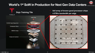
TSMC is taking the wafer-scale fabrication battle into the third dimension with a new technology. At its North American Technology Symposium, the company introduced its next-generation system-on-wafer platform—CoW-SoW—that will enable 3D integration with wafer-scale designs. This builds on the InFO_SoW system-on-wafer integration technology technology that TSMC introduced in 2020, which lets it build wafer-scale logic processors. So far, only Tesla has adopted this tech for its Dojo supercomputer, which TSMC says is now in production.
台積電正在利用新技術將晶圓級製造之戰帶入三維。在北美技術研討會上,該公司推出了下一代晶圓系統平台 CoW-SoW,該平台將實現與晶圓級設計的 3D 整合。該技術建立在台積電 2020 年推出的 InFO_SoW 晶圓級系統整合技術的基礎上,使其能夠建構晶圓級邏輯處理器。到目前為止,只有特斯拉在其 Dojo 超級電腦中採用了這項技術,台積電錶示該電腦現已投入生產。
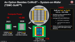
In its forthcoming CoW-SoW platform, TSMC will merge two of its packaging methods — InFO_SoW and System on Integrated Chips (SoIC) — into its system-on-wafer platform. Using the Chip-on-Wafer (CoW) tech will enable the stacking of memory or logic directly atop a system-on-wafer. The new CoW_SoW technology is expected to be ready for large-scale production by 2027, though it remains to be seen when actual products arrive on the market.
在即將推出的 CoW-SoW 平台中,台積電將把兩種封裝方法——InFO_SoW 和整合式晶片系統 (SoIC)——合併到其晶圓系統平台中。使用晶圓晶片 (CoW) 技術將能夠將記憶體或邏輯直接堆疊在晶圓系統之上。新的CoW_SoW技術預計將在2027年實現大規模生產,但實際產品何時上市仍有待觀察。
"In the future, using wafer-level integrations [will allow] our customers to integrate even more logic and memory together," said Kevin Zhang, Vice President of Business Development at TSMC. "SoW is no longer a fiction; this is something we already work with our customers [on] to produce some of the products already in place. We think by leveraging our advanced wafer-level integration technology, we can provide our customer a very important path that allows them to continue to grow their capability to bring in more computation, more energy efficient computation, to their AI cluster or [supercomputer]."
「未來,使用晶圓級整合[將允許]我們的客戶將更多的邏輯和記憶體整合在一起,」台積電業務開發副總裁 Kevin 張表示。 「SoW 不再是虛構的;我們已經與客戶合作生產一些已經到位的產品。我們認為,透過利用我們先進的晶圓級整合技術,我們可以為客戶提供非常重要的產品使他們能夠繼續增強能力,為他們的人工智慧叢集或[超級電腦]引入更多計算、更節能的計算。
Currently, TSMC's CoW-SoW focuses on integrating wafer-scale processors with HBM4 memory. These next-generation memory stacks will feature a 2048-bit interface, which will make it feasible to integrate HBM4 directly on top of logic chips. Meanwhile, it may also make sense to stack additional logic on wafer-scale processors to optimize costs.
目前,台積電的CoW-SoW專注於將晶圓級處理器與HBM4記憶體整合。這些下一代記憶體堆疊將採用 2048 位元接口,這使得將 HBM4 直接整合在邏輯晶片頂部成為可能。同時,在晶圓級處理器上堆疊額外的邏輯以優化成本也可能是有意義的。
Wafer-scale processors in general (i.e., Cerebras's WSE), and InFO_SoW-based processors in particular, offer significant performance and efficiency benefits, including high-bandwidth and low-latency core-to-core communications, low power delivery network impedance, and high energy efficiency. As an added bonus, such processors also have additional redundancy in the form of 'extra' cores.
一般而言,晶圓級處理器(即Cerebras 的WSE),特別是基於InFO_SoW 的處理器,可提供顯著的性能和效率優勢,包括高頻寬和低延遲的核心到核心通訊、低功率傳輸網絡阻抗以及高能源效率。作為額外的好處,此類處理器還具有「額外」核心形式的額外冗餘。
However, the InFO_SoW technology has certain limitations. For instance, wafer-scale processors made using this method rely entirely on on-chip memory, which may fall short for future AI needs (but is good for now). CoW-SoW will solve this, as it will allow putting HBM4 on such wafers. In addition, InFO_SoW wafers are processed using a single node, and this node does not support 3D stacking, which will be supported by CoW-SoW products.
然而,InFO_SoW技術有一定的限制。例如,使用這種方法製造的晶圓級處理器完全依賴片上記憶體,這可能無法滿足未來人工智慧的需求(但目前來說很好)。 CoW-SoW 將解決這個問題,因為它將允許將 HBM4 放置在此類晶圓上。此外,InFO_SoW晶圓採用單節點加工,該節點不支援3D堆疊,而CoW-SoW產品將支援3D堆疊。