The Memory Wall: Past, Present, and Future of DRAM
记忆墙:DRAM 的过去、现在与未来
Winners & Losers in the 3D DRAM Revolution
3D DRAM 革命中的赢家与输家
The world increasingly questions the death of Moore’s Law, but the tragedy is that it already died over a decade ago with 0 fanfare or headlines. The focus is generally on logic, but Moore’s Law always also applied to DRAM.
世界越来越质疑摩尔定律的消亡,但悲剧在于它早在十多年前就已经悄然死去,没有任何轰动或头条新闻。人们通常关注逻辑,但摩尔定律同样适用于 DRAM。
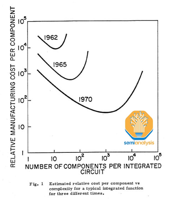
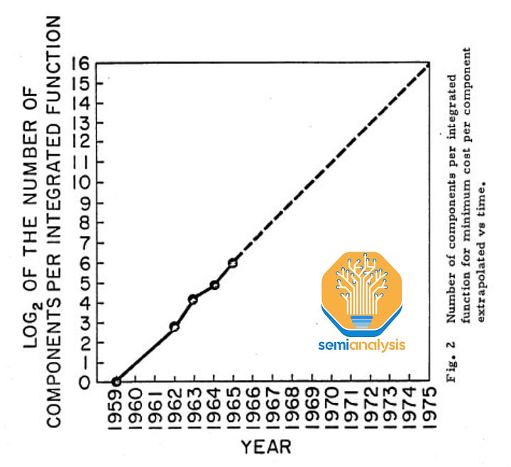
原始缩放法则 - 来源:1965 年《集成电子的未来》- 戈登·摩尔
DRAM doesn’t scale anymore. In the glory days, memory bit density doubled every 18 months – outpacing even logic. That translates to just over 100x density increase every decade. But in this last decade, scaling has slowed so much that density has increased just 2x.
DRAM 不再扩展。在辉煌的日子里,内存位密度每 18 个月翻一番——甚至超过逻辑。那意味着每十年密度增加超过 100 倍。但在过去的十年里,扩展速度减缓,密度仅增加了 2 倍。
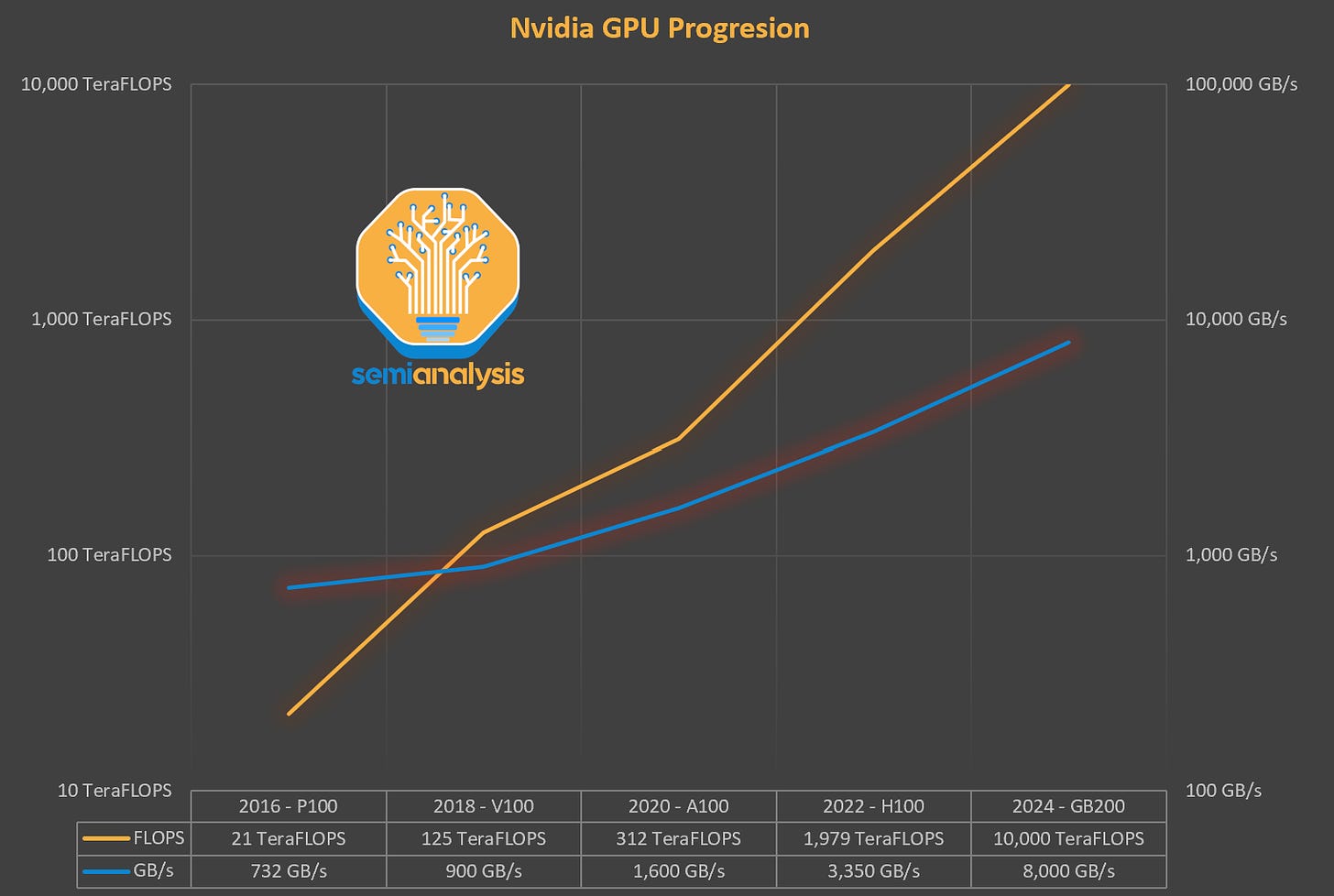
Now with the explosion in AI, the balance of the industry has been upset even further. While logic chips have improved significantly in both density and cost per transistor function over time, improvements in DRAM speeds have been slow. Despite significant FUD, the cost per transistor continues to fall on TSMC’s 3nm and 2nm nodes. While with memory, the increased bandwidth is driven by heroic and expensive packaging.
现在随着人工智能的爆炸性发展,行业的平衡进一步被打破。尽管逻辑芯片在密度和每个晶体管功能的成本上随着时间的推移有了显著改善,但 DRAM 速度的提升却相对缓慢。尽管存在显著的恐惧、不确定性和怀疑,台积电的 3nm 和 2nm 节点每个晶体管的成本仍在下降。而在内存方面,带宽的增加则是由昂贵且复杂的封装驱动的。
High bandwidth memory (HBM), the backbone of accelerator memory, costs 3x or more per GB than standard DDR5. Customers are forced to accept this as there is little alternative if they want to make a competitive accelerator package. This equilibrium is unstable – future HBM generations continue to grow even more complex with higher layer counts. AI memory needs are exploding as model weights alone approach multi-TB-scale. For the H100, ~50%+ of the cost of manufacturing is attributed to HBM and with Blackwell, this grows to ~60%+.
高带宽内存(HBM),加速器内存的支柱,其每 GB 成本是标准 DDR5 的 3 倍或更多。客户被迫接受这一点,因为如果他们想要制造具有竞争力的加速器包,几乎没有其他选择。这种平衡是不稳定的——未来的 HBM 世代将继续变得更加复杂,层数也在增加。人工智能内存的需求正在激增,仅模型权重就接近多 TB 规模。对于 H100,制造成本的~50%+归因于 HBM,而在 Blackwell 中,这一比例增长到~60%+。
The DRAM industry, in other words, has hit a wall. Compute improvements, although slowing, are vastly outpacing memory. How can the pace of innovation reaccelerate in DRAM – and what innovations can be harnessed to improve bandwidth, capacity, cost, and power use in the future?
DRAM 行业,换句话说,已经遇到了瓶颈。尽管计算性能的提升在放缓,但仍远远超过了内存。如何才能重新加速 DRAM 的创新步伐——未来可以利用哪些创新来提高带宽、容量、成本和功耗?
There are many possible solutions. With hundreds of billions in AI capex on the table, there is a strong incentive for the industry to push these solutions forward.
有许多可能的解决方案。随着数千亿的人工智能资本支出在桌面上,行业推动这些解决方案向前发展的动力很强。
Starting with a primer on the background and history of DRAM, we’ll cover each problem comprising the modern “memory wall” and possible solutions. We’ll discuss relatively simpler, short-term ideas such as extending the HBM roadmap and more complex, long-term options such as compute-in-memory (CIM), new memory types like ferroelectric RAM (FeRAM) or magnetic RAM (MRAM), and the pending arrival of 4F2 DRAM and 3D DRAM.
从 DRAM 的背景和历史入手,我们将讨论构成现代“内存墙”的每个问题及可能的解决方案。我们将讨论相对简单的短期想法,例如延长 HBM 路线图,以及更复杂的长期选项,如内存计算(CIM)、新型内存类型如铁电 RAM(FeRAM)或磁性 RAM(MRAM),以及即将到来的 4F2 DRAM 和 3D DRAM。
DRAM Primer: Working Memory
DRAM 基础知识:工作内存
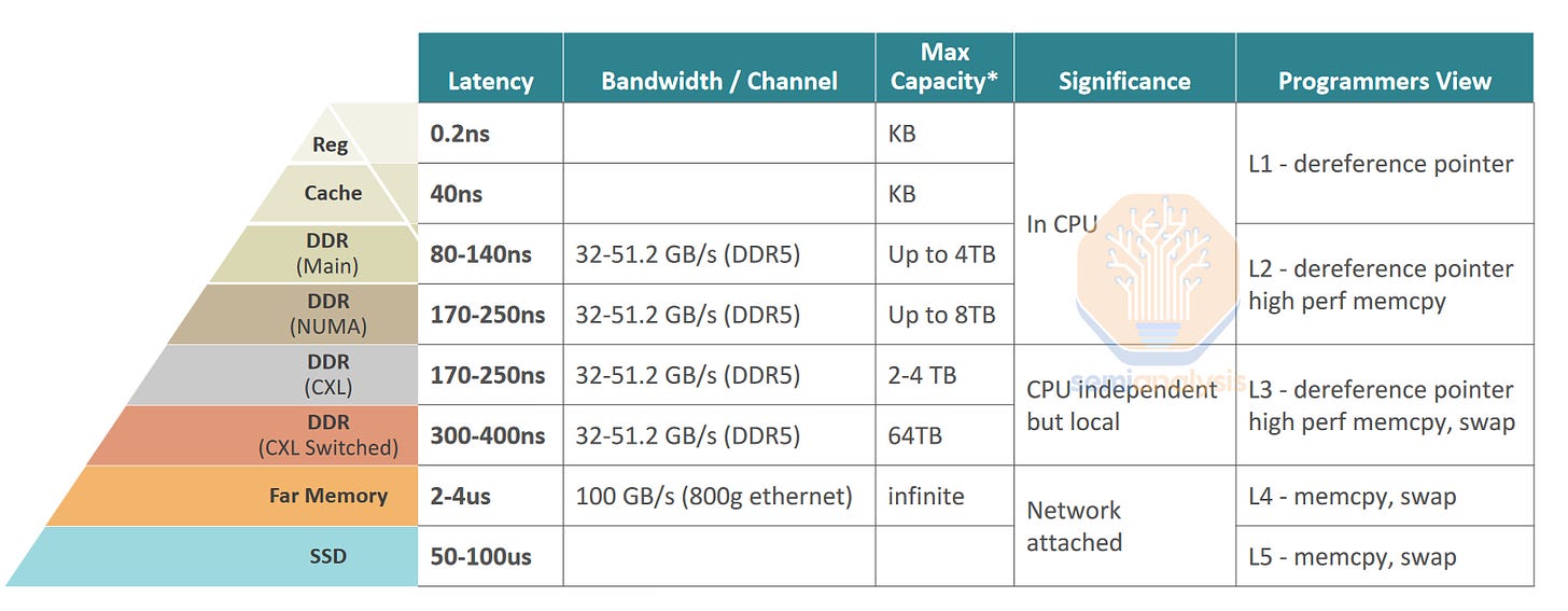
There are several types of memory used in a computer. The fastest is SRAM (Static Random Access Memory) which is compatible with logic process technologies and located on the CPU or GPU. Because it is on a logic die, SRAM is also the most expensive type of memory – about 100x+ more expensive per byte than dynamic random access memory (DRAM) – and is therefore used only in small quantities. The opposite end of the spectrum is includes non-volatile NAND solid-state drives, hard-disk drives, and magnetic tape. These are cheap but too slow for many tasks. DRAM sits in the “goldilocks” zone between SRAM and Flash – just fast enough, just cheap enough.
计算机中使用了几种类型的内存。最快的是 SRAM(静态随机存取存储器),它与逻辑工艺技术兼容,并位于 CPU 或 GPU 上。由于它位于逻辑芯片上,SRAM 也是最昂贵的内存类型——每字节的成本比动态随机存取存储器(DRAM)高出约 100 倍以上,因此仅在少量中使用。光谱的另一端包括非易失性 NAND 固态硬盘、硬盘驱动器和磁带。这些便宜,但对于许多任务来说速度太慢。DRAM 位于 SRAM 和 Flash 之间的“恰到好处”区域——速度刚好够快,价格刚好够便宜。
DRAM can make up half the cost of a non-AI server system. Yet for the past 10 years it has been the slowest to scale of all major logic and memory. 16Gb DRAM chips were first made available in high volume 8 years ago but are still the most common today; when introduced they cost around $3 per gigabyte and peaked at nearly $5 before falling back to the $3 range in the past 12 months. Speeds are, if anything, a little slower. Power has seen the best improvement largely due to the rise of LPDDR, a packaging change that uses shorter and more efficient wires, but the bar is low here. The lack of progress in DRAM scaling is a performance and economic bottleneck holding back compute.
DRAM 可以占非 AI 服务器系统成本的一半。然而,在过去的 10 年中,它是所有主要逻辑和内存中扩展速度最慢的。16Gb DRAM 芯片在 8 年前首次大规模上市,但至今仍是最常见的;推出时每千兆字节的价格约为 3 美元,最高曾接近 5 美元,过去 12 个月又回落到 3 美元左右。速度方面,实际上稍微慢了一点。功耗的改善最好,主要得益于 LPDDR 的兴起,这是一种使用更短、更高效电线的封装变化,但这里的门槛很低。DRAM 扩展缺乏进展是一个性能和经济瓶颈,制约了计算能力。
DRAM Primer: Basic Architecture
DRAM 基础知识:基本架构
In principle, DRAM is simple. It comprises an array of memory cells laid out in a grid, each storing one bit of information. All modern DRAM uses a 1T1C cell, denoting 1 transistor and 1 capacitor. The transistor controls access to the cell, and the capacitor stores the information in the form of a small electrical charge.
原则上,DRAM 是简单的。它由一个以网格布局的存储单元阵列组成,每个单元存储一位信息。所有现代 DRAM 使用 1T1C 单元,表示 1 个晶体管和 1 个电容器。晶体管控制对单元的访问,而电容器以小电荷的形式存储信息。
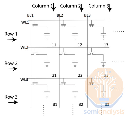
基本 DRAM 电路:一组内存单元,沿每行连接一个字线,沿每列连接一个位线。激活 1 个字线和 1 个位线可以读取或写入它们交叉的单元。
Wordlines (WL) connect all cells in a single row; they control the access transistor for each cell. Bitlines (BL) connect all cells in a single column; they connect to the source of the access transistor. When a worline is energized, the access transistors for all cells in the row open and allow current flow from the bitline into the cell (when writing to the cell) or from the cell to the BL (when reading from the cell). Only 1 worlined and 1 bitline will be active at once, meaning only the 1 cell where the active word- and bitlines intersect will be written or read.
字线(WL)连接单行中的所有单元;它们控制每个单元的访问晶体管。位线(BL)连接单列中的所有单元;它们连接到访问晶体管的源。当字线被激活时,行中所有单元的访问晶体管打开,允许电流从位线流入单元(写入单元时)或从单元流向位线(读取单元时)。一次只有 1 条字线和 1 条位线处于激活状态,这意味着只有在激活的字线和位线交叉的单元会被写入或读取。
Charge is allowed to flow from bitline to capacitor or vice versa when the access transistor is turned on by the wordline Source: Branch Education
当字线使能访问晶体管时,电荷可以从位线流向电容器或反之
DRAM is a volatile memory technology: the storage capacitors leak charge, and thus require frequent refreshes (as often as every ~32 milliseconds) to maintain stored data. Each refresh reads the contents of a cell, boosts the voltage on the bitline to an ideal level, and lets that refreshed value flow back into the capacitor. Refreshes happen entirely inside the DRAM chip, with no data flowing in or out of the chip. This minimizes wasted power, but refreshes can still come to 10%+ of total DRAM power draw.
DRAM 是一种易失性存储器技术:存储电容会漏电,因此需要频繁刷新(每约 32 毫秒一次)以维持存储数据。每次刷新都会读取单元的内容,将位线上的电压提升到理想水平,然后让刷新后的值流回电容。刷新完全在 DRAM 芯片内部进行,没有数据进出芯片。这最小化了浪费的电力,但刷新仍然可能占总 DRAM 功耗的 10%以上。
Capacitors, much like transistors, have been shrunk to nanoscopic width but also with extreme aspect ratios ~1,000nm high but only 10s of nm in diameter – aspect ratios are approaching 100:1, with capacitance on the order of 6-7 fF (femto-Farad). Each capacitor stores an extremely small charge, about 40,000 electrons when freshly written.
电容器与晶体管类似,已缩小至纳米级宽度,但也具有极端的长宽比,约为 1,000nm 高,但直径仅为几十纳米——长宽比接近 100:1,电容值在 6-7 fF(飞法拉)级别。每个电容器存储的电荷极小,刚写入时约为 40,000 个电子。
The cell must get electrons in and out via the bitline, but voltage put onto the bitline is diluted by all the other cells attached to the same bitline. Total bitline capacitance may total more than 30fF – a 5x dilution. The bitline is also very thin which slows the electrons. Finally, the cell may have drained significantly if it has not been refreshed recently, so has only a fraction of charge to deliver.
单元必须通过位线进出电子,但施加在位线上的电压会被连接到同一位线的所有其他单元稀释。总位线电容可能超过 30fF——5 倍稀释。位线也非常细,这会减慢电子的速度。最后,如果单元最近没有刷新,可能已经显著放电,因此只能提供一小部分电荷。
All these factors mean that discharging a cell to read its value can result in a very weak signal which must be amplified. To this end sense amplifiers (SA) are attached at the end of each bitline to detect the extremely small charges read from the memory cells and amplify the signal to a useful strength. These stronger signals can then be read elsewhere in the system as a binary 1 or 0.
所有这些因素意味着,放电一个单元以读取其值可能会导致非常微弱的信号,必须进行放大。为此,感应放大器(SA)被连接在每条位线的末端,以检测从存储单元读取的极小电荷,并将信号放大到有用的强度。这些更强的信号随后可以在系统的其他地方作为二进制 1 或 0 进行读取。
The sense amplifier has a clever circuit design: it compares the active bitline to a matching neighbor which is not in use, starting with both lines brought to a similar voltage. The voltage on the active bitline will be compared to the inactive neighbor, shifting the sense amp off balance and causing it to amplify the difference back into that active bitline, both amplifying the signal and driving a fresh full value, high or low, back into the cell which remains open to the bitline. It’s a 2 birds, 1 stone situation: the cell is read and refreshed at the same time.
感应放大器具有巧妙的电路设计:它将活动位线与一个未使用的匹配邻居进行比较,首先将两条线的电压调整到相似的水平。活动位线上的电压将与非活动邻居进行比较,从而使感应放大器失去平衡,并导致其将差异放大回活动位线,既放大了信号,又将一个新的完整值(高或低)驱动回仍然开放的单元。 这是一举两得的情况:单元同时被读取和刷新。
After reading/refreshing the active cell, the value can either be copied out of the chip or overwritten by a write operation. A write ignores the refreshed value and uses a stronger signal to force the bitline to match the new value. When the read or write is finished the wordlines are disabled, shutting off the access transistors and thus trapping any resident charges in the storage capacitors.
在读取/刷新活动单元后,值可以从芯片中复制出来或通过写操作覆盖。写操作会忽略刷新后的值,并使用更强的信号强制位线与新值匹配。当读取或写入完成后,字线被禁用,关闭访问晶体管,从而将任何驻留电荷困在存储电容中。
DRAM Primer: History (When DRAM Still Scaled)
DRAM 入门:历史(当 DRAM 仍在扩展时)
Modern DRAM is made possible by two separate and complementary inventions: the 1T1C memory cell, and the sense amplifier.
现代 DRAM 的实现得益于两个独立且互补的发明:1T1C 存储单元和感应放大器。
The 1T1C cell was invented in 1967 at IBM by Dr. Robert Dennard, also well known for his eponymous MOS transistor scaling law. Both DRAM and the scaling are based on MOS transistors (metal oxide silicon, the layers in the transistor gate).
1T1C 单元于 1967 年在 IBM 由罗伯特·丹纳德博士发明,他还因其同名的 MOS 晶体管缩放定律而闻名。DRAM 和缩放都基于 MOS 晶体管(氧化金属硅,晶体管栅极中的层)。
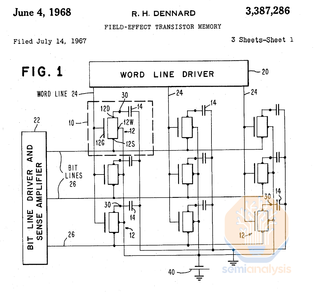
Dennard 的 1T1C 存储单元架构的原始专利。来源:美国专利 3,387,286
Despite the invention of the 1T1C memory cell structure, early DRAM shipped by Intel in 1973 used 3 transistors per cell with the gate on the middle transistor acting as a storage capacitor. This was a “gain cell” where the middle and final transistor provided gain to amplify the very small charge on the middle gate, enabling the cell to be read easily and without disturbing the stored value.
尽管 1T1C 存储单元结构已经发明,英特尔在 1973 年出货的早期 DRAM 仍然使用每个单元 3 个晶体管,中间晶体管的栅极充当存储电容。这是一个“增益单元”,其中中间和最后的晶体管提供增益,以放大中间栅极上非常小的电荷,使得单元能够轻松读取而不干扰存储值。
A 1T1C cell is better in theory: fewer devices, simpler to wire together, and smaller. Why was it not immediately adopted? It was not yet practical to read the cell.
1T1C 单元在理论上更好:设备更少,连接更简单,体积更小。为什么没有立即被采用?因为当时读取单元还不够实用。
At the time of invention, the small capacitance of the 1T1C cell made it infeasible to operate. A second key invention was needed: the sense amplifier.
在发明之时,1T1C 单元的小电容使其无法正常工作。需要第二个关键发明:传感放大器。
The first modern sense amplifier was developed in 1971 by Karl Stein at Siemens, presented at a conference in California, and completely overlooked. The 1T1C architecture was not widely adopted at that point and Siemens had no idea what to do with this invention. Stein was moved to another assignment where he had a successful career unrelated to DRAM.
第一款现代意义上的放大器于 1971 年由卡尔·施泰因在西门子开发,在加利福尼亚的一次会议上展示,但完全被忽视。1T1C 架构当时并未被广泛采用,西门子也不知道如何处理这一发明。施泰因被调往另一个岗位,在与 DRAM 无关的领域取得了成功的职业生涯。
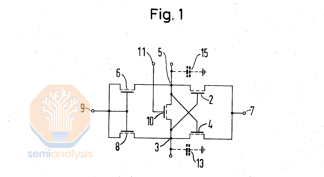
斯坦的原始信号放大器专利。来源:美国专利 3,774,176
This design was well matched to the spacing of the bit lines and has been able to scale smaller to keep pace with cell size. The sense amp is completely powered down when not in use which allows there to be millions of them on a chip without draining power. They have been a small miracle.
该设计与位线的间距非常匹配,并且能够缩小以跟上单元大小。当不使用时,感应放大器完全断电,这使得在芯片上可以有数百万个而不会耗电。它们简直是一个小奇迹。
It took more than 5 years for the sense amplifier’s time to come. Robert Proebsting at Mostek independently (re)discovered the concept and by 1977 their 16kb DRAM with 1T1C + SA architecture became the market leader. This winning formula stuck – DRAM architecture is fundamentally the same nearly 5 decades later.
感应放大器的时机来临花费了超过 5 年的时间。Mostek 的 Robert Proebsting 独立(重新)发现了这一概念,到 1977 年,他们的 16kb DRAM 采用 1T1C + SA 架构成为市场领导者。这一成功公式一直保持不变——DRAM 架构在近五十年后基本上是相同的。
DRAM Primer: When DRAM Stopped Scaling
DRAM 基础知识:当 DRAM 停止扩展时
In the 20th century, Moore’s Law and Dennard scaling ruled the semiconductor industry. At its zenith, DRAM density increases outpaced logic. DRAM capacity per chip doubled every 18 months, fueling the rise of Japanese fabs (who first exceeded US market share in 1981 and peaked around 80% in 1987) and later Korean companies (whose market share surpassed Japan’s in 1998). The rapid generational replacement of fabs on a relatively simple process created opportunities for new entrants with the funds to build the next generation fab.
在 20 世纪,摩尔定律和丹纳德缩放主导了半导体行业。在其巅峰时期,DRAM 密度的增长速度超过了逻辑电路。每个芯片的 DRAM 容量每 18 个月翻一番,推动了日本晶圆厂的崛起(他们在 1981 年首次超过美国市场份额,并在 1987 年达到约 80%的峰值)以及后来的韩国公司(其市场份额在 1998 年超过了日本)。相对简单工艺的快速代际更替为有资金建设下一代晶圆厂的新进入者创造了机会。
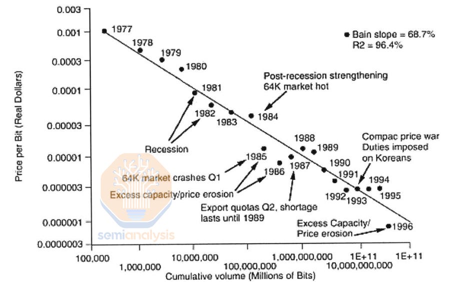
每比特价格在 20 年的“黄金时代”中降低了三个数量级,期间 DRAM 规模不断扩大。来源:Lee, K.H.,《2000 年后 DRAM 行业的战略分析》
This pace was not feasible for long, and by the end of the 20th century into the 21st, logic had outpaced memory scaling significantly. Recent logic scaling has slowed to a pace of 30-40% density improvements every 2 years. But this is still good in comparison to DRAM which is roughly an order of magnitude slower than its peak, now needing 10 years for a 2x density increase.
这种速度无法持续太久,到 20 世纪末进入 21 世纪时,逻辑的扩展速度显著超过了内存的扩展速度。最近的逻辑扩展速度已减缓至每两年 30-40%的密度提升。但与 DRAM 相比,这仍然是好的,因为 DRAM 的速度大约比其峰值慢一个数量级,现在需要 10 年才能实现 2 倍的密度增加。
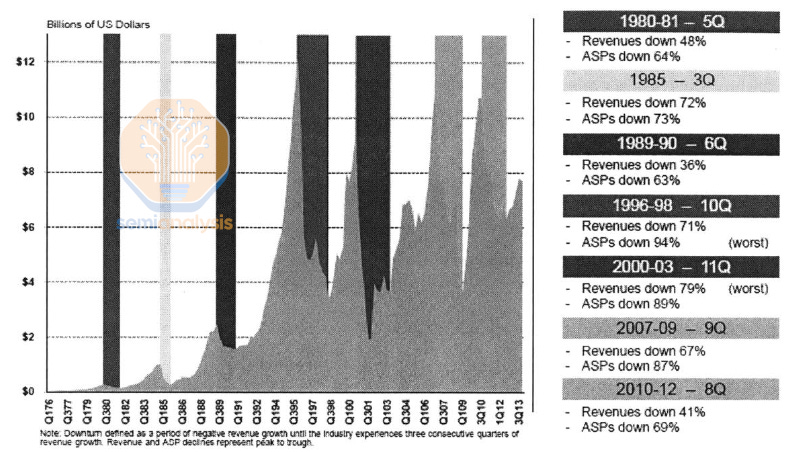
“这次不同”:不,记忆周期已经是这个行业的一部分达 50 年。来源:李,K.H.,2000 年后 DRAM 行业的战略分析
This scaling slowdown had knock-on effects in DRAM pricing dynamics. While memory has traditionally been a cyclical industry, slow density scaling has meant much less cost reduction to cushion price increases when supply is limited. The only way to increase DRAM supply is to build new fabs. Wild price swings and high CAPEX mean only the largest companies survive: more than 20 manufacturers produced DRAM in the mid 1990s, with 80% market share spread amongst the top 10. Now the top 3 suppliers own more than 95% of the market.
这种规模放缓对 DRAM 定价动态产生了连锁反应。虽然内存行业传统上是一个周期性行业,但缓慢的密度缩放意味着在供应有限时,成本降低的幅度大大减少,从而无法缓冲价格上涨。增加 DRAM 供应的唯一方法是建设新的晶圆厂。剧烈的价格波动和高资本支出意味着只有最大的公司才能生存:在 1990 年代中期,超过 20 家制造商生产 DRAM,前 10 名公司占据了 80%的市场份额。现在,前三大供应商拥有超过 95%的市场。
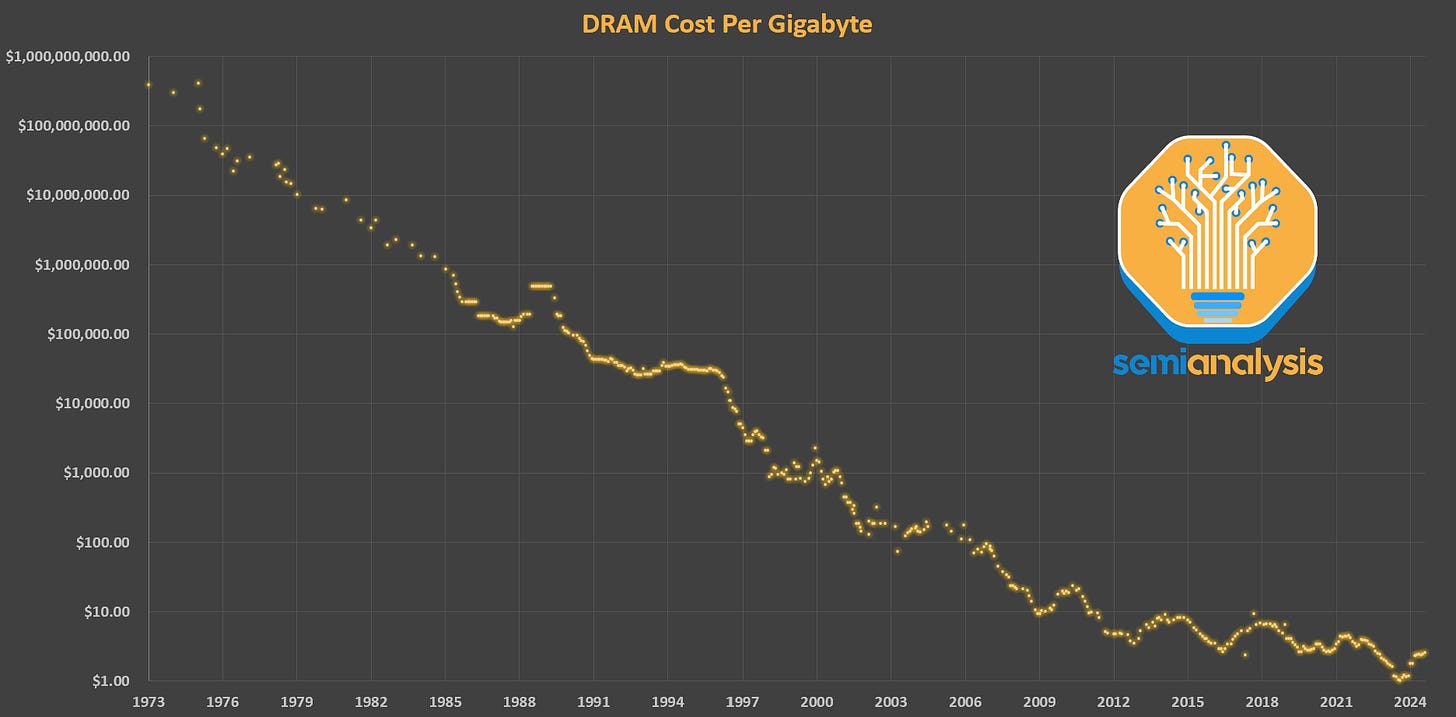
Because DRAM is commoditized, suppliers are inherently much more susceptible to price fluctuations (in contrast to logic or analog) and must compete primarily on the raw prices of their goods when the market is low. Logic has only maintained Moore’s Law with increasing costs, DRAM does not have that luxury. The cost of DRAM is simple to measure, $/Gb. Relative to earlier periods, the last 10 years have seen a slow price decrease – only 1 order of magnitude in a decade when it used to take half that time. The characteristic peak and trough behavior of DRAM is evident as well.
由于 DRAM 已经商品化,供应商本质上更容易受到价格波动的影响(与逻辑或模拟电路相比),并且在市场低迷时必须主要在商品的原始价格上竞争。逻辑电路仅以不断增加的成本维持摩尔定律,而 DRAM 没有这样的奢侈。DRAM 的成本易于测量,单位为$/Gb。与早期时期相比,过去 10 年价格缓慢下降——在十年内仅下降了一个数量级,而以前只需半个时间。DRAM 的特征性峰谷行为也很明显。
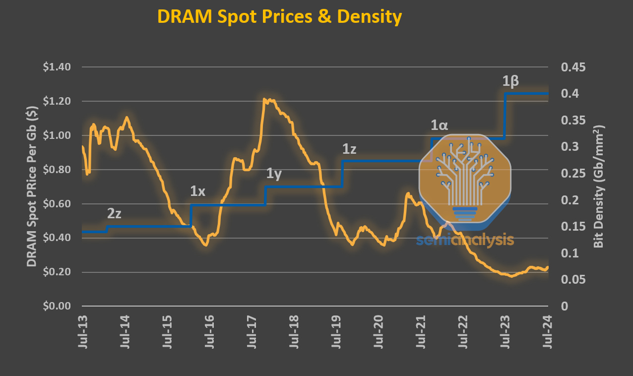
DRAM 密度缩放速度减缓至每十年 2 倍,而价格受周期性影响驱动。来源:DRAMExchange,SemiAnalysis
Since entering the 10-nm nodes, DRAM bit density has stagnated. Even the addition of EUV in Samsung’s 1z and SK Hynix’s 1a nodes did not significantly increase density. Two notable challenges are in the capacitors and sense amplifiers.
自进入 10 纳米节点以来,DRAM 位密度停滞不前。即使在三星的 1z 节点和 SK 海力士的 1a 节点中加入了 EUV,也未能显著提高密度。两个显著的挑战在于电容器和信号放大器。
Capacitors are difficult in many aspects. First, patterning is demanding as the holes must be tightly packed with very good critical dimension (CD) and overlay control, to contact the access transistors below and avoid bridging or other defects. Capacitors have a very high aspect ratio and etching a straight and narrow hole profile is exceptionally difficult, further compounded by the need for a thicker hardmask to enable a deeper etch as a thicker mask necessitates thicker photoresist which is harder to pattern.
电容器在许多方面都很困难。首先,图案化要求很高,因为孔必须紧密排列,具有非常好的关键尺寸(CD)和叠加控制,以接触下面的接入晶体管,并避免桥接或其他缺陷。电容器具有非常高的纵横比,刻蚀直且窄的孔型极其困难,进一步加剧了需要更厚的硬掩膜以实现更深刻蚀的需求,因为更厚的掩膜需要更厚的光刻胶,而这更难以图案化。
Next, multiple defect-free layers of a few nm thickness must be deposited on the walls throughout the hole profile to form the capacitor. Nearly every step strains the limits of modern processing technology.
接下来,必须在孔型的墙壁上沉积多个无缺陷的几纳米厚的层,以形成电容器。几乎每一步都在挑战现代加工技术的极限。
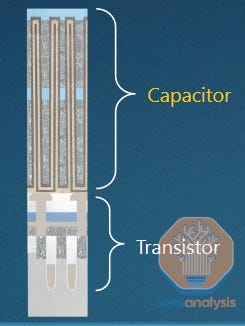
DRAM 存储电容器需要在 100:1 的纵横比孔中形成许多精致的层(不按比例 - 实际电容器可能比所示高 10 倍)。来源:应用材料公司
Sense amplifiers are a similar story to logic interconnects. Once an afterthought, they are now of equal or even greater difficulty than the “main” features (logic transistors and memory cells). They are squeezed from multiple sides. Area scaling must be done to match bitline shrink, with the sense amps becoming less sensitive and more prone to variation and leakage as they are made smaller. At the same time, smaller capacitors store less charge, so the sensing requirement to read them becomes more difficult.
感应放大器的情况与逻辑互连类似。曾经被视为附属品的它们,现在与“主要”特性(逻辑晶体管和存储单元)同样甚至更具挑战性。它们受到多方面的挤压。必须进行面积缩放以匹配位线缩小,随着感应放大器变小,它们的灵敏度降低,更容易受到变化和泄漏的影响。同时,更小的电容器存储的电荷更少,因此读取它们的感应要求变得更加困难。
There are other challenges as well, with the upshot being that scaling DRAM in an economical way is increasingly difficult using traditional approaches. The door is open for new ideas – let’s explore some of them…
还有其他挑战,结果是以经济的方式扩展 DRAM 使用传统方法变得越来越困难。新思路的机会已经打开——让我们来探索其中的一些……
Short-Term Scaling: 4F2 and Vertical Channel Transistor
短期扩展:4F2 和垂直通道晶体管
In the short-term, DRAM scaling will continue along its traditional roadmap. Larger, fundamental changes to architecture will take years to develop and implement. In the meantime, the industry must respond to the need for better performance, even if only with marginal improvements.
在短期内,DRAM 的缩放将继续沿着其传统路线图发展。架构的更大、根本性的变化将需要数年才能开发和实施。与此同时,行业必须响应对更好性能的需求,即使只是通过边际改进。
The short-term roadmap has 2 innovations: the 4F2 cell layout and vertical channel transistors (VCT).
短期路线图有两个创新:4F2 单元布局和垂直通道晶体管(VCT)。
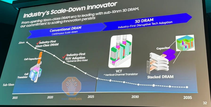
三星 DRAM 路线图。来源:三星 Memcon 2024,最初由 SemiEngineering 发布
Note that some companies, including Samsung in their roadmap, put VCT under the “3D” banner. While technically true, this is a bit misleading as VCT is distinct from what is commonly called “3D DRAM.”
请注意,包括三星在内的一些公司在其路线图中将 VCT 归类于“3D”类别。虽然从技术上讲这是正确的,但这有点误导,因为 VCT 与通常所称的“3D DRAM”是不同的。
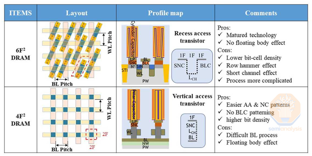
标准的 6F2 布局与 4F2 垂直通道晶体管。来源:CXMT IEDM 2023
4F2 describes the memory cell area in terms of the minimum feature size F, similar to the track metric for standard logic cell height e.g. a “6T cell.” The minimum feature size is generally the line or space width, in DRAM this will be the wordline or bitline width. It’s a simple way to denote the density of a cell layout and makes comparison easy – a 4F2 cell is only 2/3rds the size of a 6F2 cell, offering a theoretical 30% density increase without scaling the minimum feature size. Note that pure cell layout is not the only limit to density scaling, so the real benefits are likely to be less than the ideal 30% case.
4F2 用最小特征尺寸 F 来描述存储单元面积,类似于标准逻辑单元高度的轨道度量,例如“6T 单元”。最小特征尺寸通常是线或间距宽度,在 DRAM 中,这将是字线或位线宽度。这是一种简单的方式来表示单元布局的密度,并使比较变得容易——4F2 单元的大小仅为 6F2 单元的 2/3,提供了理论上 30% 的密度增加,而无需缩放最小特征尺寸。请注意,纯单元布局并不是密度缩放的唯一限制,因此实际收益可能低于理想的 30% 情况。
4F2 is the theoretical limit for a single bit cell. Recall that feature size is the line or space width (i.e. the half pitch), so a line + space pattern will have a pitch of 2F, not F, and thus the minimum possible cell size is 4F2 not just F2. So once this architecture is achieved, the only avenue for horizontal scaling is to scale F itself – something that is rapidly becoming impractical, if not outright impossible.
4F2 是单比特单元的理论极限。请记住,特征尺寸是线或间距宽度(即半间距),因此线 + 间距模式的间距为 2F,而不是 F,因此最小可能的单元大小是 4F2,而不仅仅是 F2。因此,一旦实现这种架构,水平扩展的唯一途径就是扩展 F 本身——这正迅速变得不切实际,甚至完全不可能。
DRAM has used a 6F2 layout since 2007, with 8F2 before that (interesting aside: modern NAND already uses a 4F2 cell but with a significantly larger feature size F. SRAM is on the order of 120 F2, 20x less dense!)
自 2007 年以来,DRAM 采用了 6F2 布局,此前为 8F2(有趣的是:现代 NAND 已经使用 4F2 单元,但特征尺寸 F 显著更大。SRAM 的密度约为 120 F2,低 20 倍!)
One notable exception is CXMT, a Chinese vendor which used VCTs and a 4F2 layout in their sanctions busting 18-nm DRAM, demonstrated in late 2023. Because Samsung, SK Hynix, and Micron were able to scale cells, they were not forced to adopt these architectures in the same way that CXMT was. The implication of CXMT’s early adoption is also important – it is likely they are having difficulty scaling F as they opted for the more drastic change in cell and transistor architectures.
一个显著的例外是 CXMT,这是一家中国供应商,他们在 2023 年底展示了其用于规避制裁的 18 纳米 DRAM,采用了 VCT 和 4F2 布局。由于三星、SK 海力士和美光能够扩展单元,因此他们并没有像 CXMT 那样被迫采用这些架构。CXMT 早期采用的含义也很重要——他们可能在扩展 F 方面遇到了困难,因为他们选择了更为激进的单元和晶体管架构的变化。
The key enabler for 4F2 cells is the vertical channel transistor. It’s necessary simply because the transistor must scale down to fit in the cell and both contacts – to bitline and to capacitor – must also fit in that footprint, so, one vertical line. At these scales it becomes necessary to construct the transistor vertically instead of horizontally, reducing its footprint down to roughly 1F, roughly matching the capacitor above it, while maintaining enough channel length for the transistor to operate effectively. Current DRAM uses horizontal channels and source/drains with horizontal separation. These are a mature and well understood architecture. VCTs stack a source (connected to the BL below it), channel (surrounded by gate & the wordline controlling the gate), and drain (connected to the capacitor above) sequentially. There are tradeoffs in fabrication where some steps get easier and others harder, but overall VCTs are more difficult to manufacture.
4F2 单元的关键推动因素是垂直通道晶体管。这是必要的,因为晶体管必须缩小以适应单元,并且两个接触点——与位线和电容器的接触——也必须适应这个占地面积,因此需要一条垂直线。在这些尺度下,构建垂直晶体管而不是水平晶体管变得必要,从而将其占地面积缩小到大约 1F,基本与其上方的电容器相匹配,同时保持足够的通道长度以使晶体管有效工作。目前的 DRAM 使用水平通道和具有水平间隔的源/漏。这是一种成熟且易于理解的架构。VCTs 依次堆叠源(连接到其下方的 BL)、通道(被栅极和控制栅极的字线包围)和漏(连接到上方的电容器)。在制造过程中存在权衡,一些步骤变得更容易,而另一些则更困难,但总体而言,VCTs 的制造更为复杂。
Samsung’s process is notable for the use of wafer bonding. In a process similar to backside power delivery for logic, the cell access transistors are fabricated with bitlines formed on top before flipping the wafer over and bonding to a support wafer, so the bitline is now buried. Interestingly, the bonded base does not seem to need accurate alignment with the VCTs though the disclosure does not explain whether the periphery CMOS will be on the flipped chip, or in the newly bonded base. The topside is thinned to expose the other end of the transistors so the storage capacitors can be built atop them. EVG and TEL stand to gain from this new incremental need for wafer bonding tools.
三星的工艺以使用晶圆键合而著称。在一种类似于逻辑电路背面供电的工艺中,单元接入晶体管是在顶部形成位线后制造的,然后将晶圆翻转并键合到支撑晶圆上,因此位线现在被埋在里面。有趣的是,尽管披露并未解释周边 CMOS 是否会在翻转的芯片上,或是在新键合的基底中,但键合基底似乎并不需要与 VCTs 进行精确对齐。顶部被削薄以暴露晶体管的另一端,以便在其上构建存储电容器。EVG 和 TEL 将从这一新增加的晶圆键合工具需求中受益。
DRAM Primer: Current Variants
DRAM 基础知识:当前变种
DRAM comes in many varieties, each optimized for different goals. The relevant latest-gen flavors are DDR5, LPDDR5X, GDDR6X, and HBM3/E. Differences between them lie almost entirely in the peripheral circuits. The memory cells themselves are similar across varieties and the fabrication methods are broadly similar for all types. Let’s briefly introduce the various DRAM flavors and the role of each.
DRAM 有多种类型,每种类型都针对不同的目标进行了优化。相关的最新一代类型包括 DDR5、LPDDR5X、GDDR6X 和 HBM3/E。它们之间的差异几乎完全在于外围电路。内存单元本身在各个类型之间相似,制造方法在所有类型中大致相似。让我们简要介绍各种 DRAM 类型及其各自的作用。
DDR5 (Double Data Rate gen. 5) delivers the highest memory capacity as it is packaged in dual in-line memory modules (DIMMs). LPDDR5X (Low Power DDR5 with X meaning enhanced) provides low-power operation but requires shorter distances and low capacitance connections to the CPU which limit capacity, so it is used in mobile phones and laptops where low power is desirable and the layout constraints tolerable.
DDR5(双倍数据速率第 5 代)提供了最高的内存容量,因为它被封装在双列直插内存模块(DIMM)中。LPDDR5X(低功耗 DDR5,X 表示增强)提供低功耗操作,但需要更短的距离和低电容连接到 CPU,这限制了容量,因此它用于手机和笔记本电脑,在这些设备中低功耗是可取的,布局限制是可以接受的。
More recently we have seen higher capacity packaging for LPDDR used in some AI accelerators, Apple’s professional workstations, and AI feeder CPUs such as Grace. These new uses are driven by the search for power efficient data transfers and high bandwidth.
最近,我们看到在一些 AI 加速器、苹果的专业工作站以及像 Grace 这样的 AI 供给 CPU 中使用了更高容量的 LPDDR 封装。这些新用途是由对高效能数据传输和高带宽的需求驱动的。
In accelerators, LPDDR has emerged as the best option for a “2nd tier” of memory that provides cheaper capacity at a lower (slower) level than expensive HBM. It falls short in building highest capacities and in reliability features, but beats DDR5 DIMMs as it consumes an order of magnitude less energy per bit of throughput. LPDDR5X packaging goes up to 480GB available on the Nvidia Grace processor, which is about 10x the capacity limit for GDDR configurations (which are limited by rules of circuit board layout and chip packaging required to meet signal in consumer gaming systems), and in the same range as medium DDR server configurations. Larger capacity DDR5 is possible using R-DIMMS of size above 128GB, albeit costly due to packaging complexity and the additional Registers (a kind of buffer chip) on the DIMMs.
在加速器中,LPDDR 已成为“二级”内存的最佳选择,它提供比昂贵的 HBM 更便宜的容量,且速度较慢。尽管在构建最高容量和可靠性特性方面有所不足,但它在每比特吞吐量的能耗上比 DDR5 DIMM 低一个数量级。LPDDR5X 封装可达到 480GB,适用于 Nvidia Grace 处理器,这大约是 GDDR 配置的容量限制的 10 倍(受限于电路板布局和芯片封装的规则,以满足消费游戏系统中的信号要求),并且与中型 DDR 服务器配置在同一范围内。使用超过 128GB 的 R-DIMMS 可以实现更大容量的 DDR5,尽管由于封装复杂性和 DIMM 上的额外寄存器(一种缓冲芯片),成本较高。
LPDDR5X has a large advantage in power consumption vs. DDR and in cost vs. HBM, but the energy per bit cannot challenge HBM and it requires many lanes (connections to the CPU) which crowd board layouts at larger capacities. It also has a weak story on error correction (ECC) which becomes more important at larger capacities as there is greater chance of an error. To compensate, some capacity must be diverted to support extra ECC. For example, the Grace CPU has 512GB of LPDDR5x per compute tray but seems to reserve 32GB for reliability features, leaving 480GB available for use.
LPDDR5X 在功耗方面相较于 DDR 具有很大优势,在成本方面相较于 HBM 也有优势,但每比特的能量无法与 HBM 竞争,并且它需要多个通道(与 CPU 的连接),在更大容量时会挤占电路板布局。此外,它在错误校正(ECC)方面表现较弱,而在更大容量时,错误发生的可能性更高,因此 ECC 变得更加重要。为了补偿,部分容量必须被分配用于支持额外的 ECC。例如,Grace CPU 每个计算托盘有 512GB 的 LPDDR5x,但似乎保留了 32GB 用于可靠性功能,剩余 480GB 可供使用。
The upcoming LPDDR6 standard shows little improvement, retaining high lane counts per chip and relatively mild speed increases along with limited support for error correction. LPDDR6 will not deliver an HBM competitor.
即将推出的 LPDDR6 标准几乎没有改进,保持每个芯片的高通道数和相对温和的速度提升,同时对错误纠正的支持有限。LPDDR6 不会提供 HBM 竞争对手。
GDDR6X (G for Graphics) is focused on graphics applications, offering high bandwidth at low cost but with higher latency and higher power consumption. Although useful in gaming GPUs, it was engineered with board-level capacity limits and power levels that limit the size of AI applications which can use it.
GDDR6X(G 代表图形)专注于图形应用,提供高带宽、低成本,但具有更高的延迟和更高的功耗。尽管在游戏 GPU 中有用,但它的设计考虑了板级容量限制和功率水平,这限制了可以使用它的 AI 应用的规模。
Then there is HBM3E (High Bandwidth Memory gen. 3, with an enhanced “E” version). It prioritizes bandwidth and power efficiency but is very expensive. The 2 defining characteristics of HBM are the much wider bus width and the vertically stacked memory die. Individual HBM die have 256 bits each of I/O, 16x more than LPDDR which has a bus width of only 16 bits per chip. Dies are vertically stacked, typically 8 or more, with I/O grouped for every 4 dies; in total the package can deliver 1024 bits of bandwidth. In HBM4 this will double to 2048 bits. To make the most of HBM it is best co-packaged next to the compute engine to reduce latency and energy per bit. To expand capacity while maintaining a short connection to compute, more dies must be added to the stack.
然后是 HBM3E(高带宽内存第 3 代,增强版“E”)。它优先考虑带宽和功率效率,但成本非常高。HBM 的两个定义特征是更宽的总线宽度和垂直堆叠的内存芯片。每个 HBM 芯片具有 256 位的 I/O,是 LPDDR 的 16 倍,而 LPDDR 的总线宽度仅为每个芯片 16 位。芯片垂直堆叠,通常为 8 个或更多,每 4 个芯片分组 I/O;总的来说,封装可以提供 1024 位的带宽。在 HBM4 中,这将增加到 2048 位。为了充分利用 HBM,最好将其与计算引擎共同封装,以减少延迟和每位的能耗。为了在保持与计算的短连接的同时扩展容量,必须向堆叠中添加更多芯片。
The high cost of HBM is mainly driven by this need for die stacking. In a typical HBM stack, 8 or 12 DRAM dies (with 16 and beyond on the roadmap) are stacked atop each other, with power and signal routed by Through Silicon Vias (TSVs) in each die. TSVs are wires passing directly through the chip, that allow connection between chips. TSVs are much denser, more performant, and more costly than the older wire-bonding methods used to connect stacked chips. More than 1,200 signal wires must be routed via TSVs in an HBM stack. Significant area must be dedicated to them, making each HBM DRAM die double the size of a standard DDR die for the same capacity. This also means higher binning requirements for electrical and thermal performance for the DRAM die.
HBM 的高成本主要是由于对芯片堆叠的需求。在典型的 HBM 堆叠中,8 或 12 个 DRAM 芯片(在路线图上有 16 个及以上)相互堆叠,电源和信号通过每个芯片中的硅通孔(TSV)进行连接。TSV 是直接穿过芯片的导线,允许芯片之间的连接。与用于连接堆叠芯片的旧线键合方法相比,TSV 的密度更高、性能更好且成本更高。在 HBM 堆叠中,必须通过 TSV 路由超过 1200 条信号线。必须为它们分配大量面积,使得每个 HBM DRAM 芯片的大小是相同容量标准 DDR 芯片的两倍。这也意味着对 DRAM 芯片的电气和热性能有更高的分选要求。
This complexity detracts from yield. For example, Samsung’s DRAM design mishaps and their use of a trailing 1α node are contributing to their shockingly poor HBM yields. Packaging is the other major challenge. Properly aligning 8+ die with thousands of connections each is difficult and therefore expensive due to relatively low yields. At the moment this is one of the key differentiators between HBM suppliers, as SK Hynix can successfully produce HBM3E with their MR-MUF packaging while Samsung struggles to yield their product. Micron has a viable solution, but needs to scale production significantly.
这种复杂性降低了产量。例如,三星的 DRAM 设计失误以及他们使用的滞后 1α节点正在导致其 HBM 产量惊人地低。封装是另一个主要挑战。正确对齐 8 个以上的芯片,每个芯片有数千个连接是困难的,因此由于相对较低的产量而成本高昂。目前,这也是 HBM 供应商之间的一个关键差异化因素,因为 SK 海力士能够成功生产 HBM3E 及其 MR-MUF 封装,而三星在产品产量上则面临困难。美光有一个可行的解决方案,但需要大幅提升生产规模。
Despite the high costs and yield challenges HBM3E is, for now, the most valuable and high-margin product the memory industry has ever had. This is primarily because for large-model AI Accelerators, no other flavor of DRAM is a viable alternative. While margins are likely to erode as Samsung improves yield, and Micron as they scale production, the memory appetite of AI accelerators will continue to grow – to some extent offsetting the benefit of this new supply.
尽管成本高昂且产量面临挑战,HBM3E 目前仍是内存行业有史以来最有价值和高利润的产品。这主要是因为对于大型模型的 AI 加速器,其他类型的 DRAM 并不是可行的替代品。虽然随着三星提高产量和美光扩大生产,利润率可能会下降,但 AI 加速器对内存的需求将继续增长,在某种程度上抵消这一新供应的好处。

HBM 在带宽和封装密度方面占据主导地位。来源:SemiAnalysis
In short, high bandwidth and very high bandwidth density along with best energy per bit and true ECC capability makes HBM3E the clear winner, for now, for AI Accelerators. This is why products like Nvidia’s H100 and AMD’s MI300X use it. GDDR6/X comes in a distant second by the same metrics albeit with tiny capacity. LPDDR5 and DDR5 are even worse, neither is suited to accelerator needs.
简而言之,高带宽和非常高的带宽密度,以及最佳的每比特能量和真正的 ECC 能力,使得 HBM3E 在目前成为 AI 加速器的明显赢家。这就是为什么像 Nvidia 的 H100 和 AMD 的 MI300X 这样的产品使用它。根据相同的指标,GDDR6/X 位居第二,尽管容量很小。LPDDR5 和 DDR5 更糟,均不适合加速器的需求。
The current HBM solution is expensive and will be increasingly difficult to scale. How did we end up in this situation?
当前的 HBM 解决方案成本高昂,并且将越来越难以扩展。我们是如何陷入这种境地的?
HBM Roadmap HBM 路线图
HBM is a packaging solution built around legacy DRAM ideas, but packaged with density and adjacency to try to solve the bandwidth and power problems for AI and other forms of high-performance computing.
HBM 是一种围绕传统 DRAM 理念构建的封装解决方案,但通过密度和邻近性进行封装,以尝试解决 AI 和其他高性能计算形式的带宽和功耗问题。
All leading AI GPUs now use HBM as their memory. Plans for 2025 have 12-Hi HBM3e with 32 Gb chips for a total of 48 GB per stack, with data rate to 8 Gbps per wire. In GPU servers the first versions of unified memory with a supporting CPU have launched with AMD’s MI300A and Nvidia’s Grace Hopper.
所有领先的 AI GPU 现在都使用 HBM 作为其内存。2025 年的计划是使用 12-Hi HBM3e,配备 32 Gb 芯片,每个堆叠总共 48 GB,数据传输速率为每根线 8 Gbps。在 GPU 服务器中,支持 CPU 的统一内存的首个版本已与 AMD 的 MI300A 和 Nvidia 的 Grace Hopper 一起推出。
The Grace CPU has high capacity LPDDR5X, while the GPU has high bandwidth HBM3. However, the CPU and GPU are on separate packages, connected over NVLink-C2C at 900 GB/s. This model is simpler to integrate but more difficult on the software side. The latency of memory connected to the other chip is much higher and could affect a significant number of workloads. As such, the memory is not quite uniform and comes with its own challenges.
Grace CPU 具有高容量的 LPDDR5X,而 GPU 则配备高带宽的 HBM3。然而,CPU 和 GPU 位于不同的封装中,通过 900 GB/s 的 NVLink-C2C 连接。该模型更易于集成,但在软件方面更具挑战性。连接到另一芯片的内存延迟较高,可能会影响大量工作负载。因此,内存并不完全均匀,并带来了自身的挑战。
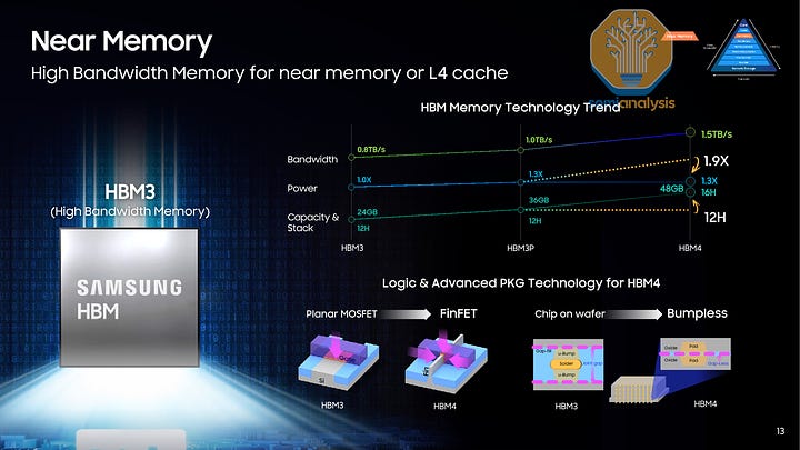
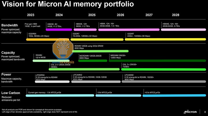
HBM4 is a few years away, with Samsung and Micron claiming it will be up to 16-Hi with 1.5 TB/s per stack. This is more than twice the bandwidth of what we have today at only 1.3-1.5x the power, but this scaling is not enough, as the power consumption of memory continues to increase overall. HBM4 will also change to 2048-bit width per stack, reducing data rates by a small amount to 7.5 Gbps, helping with power consumption and signal integrity. It is likely that the data rates will increase to the levels of HBM3E with HBM4E or something similar.
HBM4 还需要几年时间才能问世,三星和美光声称其每个堆栈将达到 16-Hi,带宽为 1.5 TB/s。这是我们今天带宽的两倍多,功耗仅增加 1.3-1.5 倍,但这种扩展仍然不够,因为内存的整体功耗持续增加。HBM4 还将改为每个堆栈 2048 位宽,数据速率略微降低至 7.5 Gbps,有助于降低功耗和信号完整性。HBM4E 或类似产品的数据显示速率可能会提高到 HBM3E 的水平。
The other significant change is in the HBM base die. The base die will be fabricated on FinFET processes as opposed to the planar CMOS technology used now. For Micron and SK Hynix who do not have this logic capability, the base die will be fabricated by a foundry with TSMC already making announcements that they will be the partner for SK Hynix. Additionally, there will be customization of the base die for individual customers.
另一个重要变化是在 HBM 基础芯片上。基础芯片将采用 FinFET 工艺制造,而不是目前使用的平面 CMOS 技术。对于没有此逻辑能力的美光和 SK 海力士,基础芯片将由代工厂制造,台积电已经宣布将成为 SK 海力士的合作伙伴。此外,基础芯片将根据个别客户的需求进行定制。
We have a separate report on HBM customization coming, but a quick primer here:
我们有一份关于 HBM 定制的单独报告即将发布,但这里简单介绍一下:
HBM4 announcements predict that at least 2 different forms of base chip will be in use, allowing the memory interface to be optimized for different speeds and lengths. It is likely that functionality controlling the DRAM state machine will move onto the base chip to more efficiently control the DRAM chips, and the vertical-only connections may allow energy per bit to be reduced.
HBM4 公告预测至少将有 2 种不同形式的基础芯片投入使用,从而使内存接口能够针对不同的速度和长度进行优化。控制 DRAM 状态机的功能可能会转移到基础芯片上,以更有效地控制 DRAM 芯片,并且仅垂直连接可能会降低每位的能耗。
Custom HBM can enable multiple other package architectures outside of the conventional CoWoS-based assemblies we see today. There could be repeater PHY to daisy chain multiple rows of HBM -though anything beyond 2 ranks would see diminishing returns.
定制的 HBM 可以支持多种其他封装架构,超出我们今天所见的传统 CoWoS 基组装。可能会有中继 PHY 来串联多个 HBM 行——尽管超过 2 个排的任何配置都会看到收益递减。
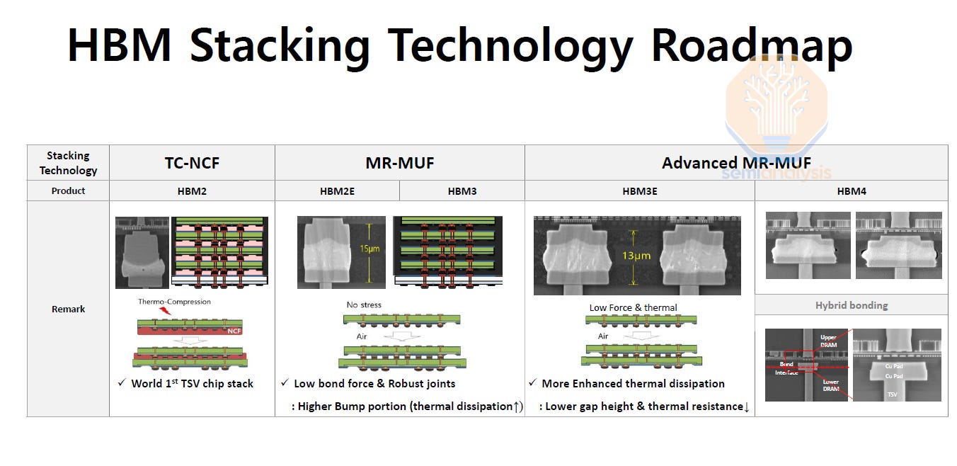
With HBM4 and successors, the move to hybrid bonding has been suggested. This will allow for thinner HBM stacks as the bump gap is removed, and improved heat dissipation. Moreover, it will allow for stack heights of 16-20+ layers. It may also reduce power consumption by a small amount as the physical distance that signals travel will be reduced. The challenges are substantial though – yielding a bonded stack of 16+ die, none perfectly flat, is not easy – nobody is close to a high volume manufacturing-ready solution here.
随着 HBM4 及其后续产品的推出,建议采用混合键合。这将允许更薄的 HBM 堆叠,因为凸点间隙被去除,并改善热散逸。此外,它将允许 16-20 层以上的堆叠高度。它还可能在一定程度上减少功耗,因为信号传输的物理距离将缩短。然而,挑战是相当大的——获得一个由 16 个以上芯片键合而成的堆叠,且没有一个完全平坦,并不容易——在这里没有人接近高产量制造就绪的解决方案。
All initial HBM4 will not use hybrid bonding, and we expect that to remain true for much longer than most would hope.
所有初始的 HBM4 将不会使用混合键合,我们预计这种情况将持续比大多数人希望的时间更长。
The connection between the CPU, GPU or accelerator, and memory is in the base chip. Improving this connection is one possible avenue for overcoming memory limitations. Eliyan, a startup funded by Micron and Intel amongst others, is spearheading this approach with their UMI custom interface.
CPU、GPU 或加速器与内存之间的连接位于基础芯片中。改善这种连接是克服内存限制的一个可能途径。Eliyan,一家获得美光和英特尔等公司资助的初创公司,正在通过他们的 UMI 定制接口引领这一方法。
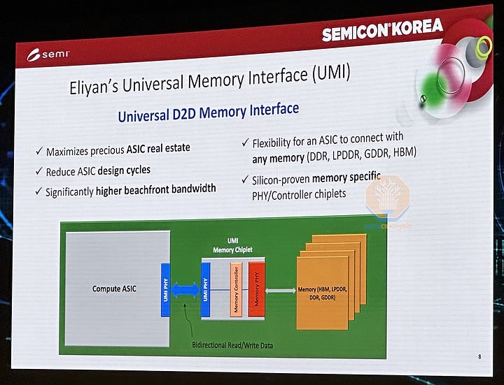
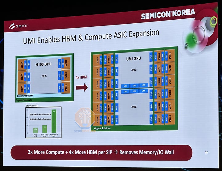
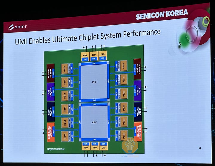
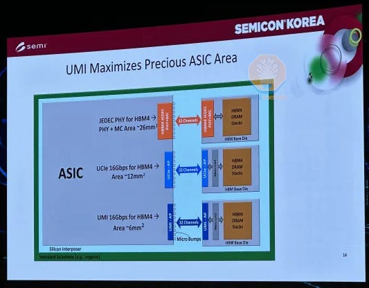
This UMI interface is used with an ASIC die, which acts as the base chip for an HBM stack or a module controller for other memory types. This chiplet contains both the memory controller and physical interconnect (PHY) to the memory chips. The UMI connects externally to the host GPU, attaching to the fabric of the host. Manufactured with a full CMOS process they can be fast and efficient, using an advanced “Nulink” protocol to connect to the host and eliminate the memory controller footprint from the host silicon.
该 UMI 接口与 ASIC 芯片一起使用,作为 HBM 堆栈的基础芯片或其他内存类型的模块控制器。该芯片包含内存控制器和与内存芯片的物理互连(PHY)。UMI 外部连接到主机 GPU,附加到主机的结构上。采用全 CMOS 工艺制造,它们可以快速高效,使用先进的“Nulink”协议连接到主机,并消除主机硅片上的内存控制器占用空间。
Eliyan’s packaging technologies work even with standard substrates and have much further reach than regular advanced packaging. This may allow for HBM that is not adjacent to the ASIC die, but much further away, meaning higher capacities can be accommodated. Their approach also uses less area and shoreline on the host which means that the channel width can be increased. Standardized UMI memory chiplets could allow for HBM, DDR, CXL memory and more to be used without being fixed to a specific type, increasing flexibility significantly. While it’s possible this approach may offer short-term improvements, it does not address the underlying cost issues with HBM.
Eliyan 的封装技术即使在标准基板上也能正常工作,其覆盖范围远超常规先进封装。这可能允许 HBM 不与 ASIC 芯片相邻,而是远离,这意味着可以容纳更高的容量。他们的方法还使用了更少的面积和边界,这意味着通道宽度可以增加。标准化的 UMI 内存芯片组可以允许 HBM、DDR、CXL 内存等的使用,而不固定于特定类型,从而显著提高灵活性。虽然这种方法可能在短期内提供改进,但并未解决 HBM 的根本成本问题。
Emerging Memory 新兴记忆
For as long as DRAM and NAND have been incumbent, there has been research into better alternatives. The umbrella term for these is “emerging memories.” It’s a bit of a misnomer as, so far, none of them have managed to “emerge” into a high volume product. Given the new challenges and incentives surrounding AI though, they’re worth at least a short discussion.
自从 DRAM 和 NAND 占据市场以来,就一直在研究更好的替代品。这些替代品的统称是“新兴存储器”。这个名称有些不准确,因为到目前为止,它们都未能“浮现”成高产量产品。不过,考虑到围绕人工智能的新挑战和激励,它们至少值得进行简短讨论。
The most promising memory for discrete applications is FeRAM. Instead of using a dielectric (insulating material) in the storage capacitor, they use a ferroelectric (a material that polarizes in an electric field). These have the desirable characteristic of being non-volatile i.e. they can store data when turned off and do not waste power or time on refreshes.
最有前景的离散应用内存是 FeRAM。它们在存储电容器中使用的是铁电材料(在电场中极化的材料),而不是介电材料(绝缘材料)。这些材料具有非易失性的理想特性,即在关闭时可以存储数据,并且不会浪费电力或时间进行刷新。
Micron showed promising results at IEDM 2023 with density comparable to their D1β DRAM along with good endurance and retention performance. In other words a good candidate for AI/ML use if it weren’t for one issue: cost. It is complex to manufacture and makes more use of exotic materials than conventional DRAM, to the point that it simply is not competitive at present.
美光在 2023 年 IEDM 上展示了有前景的结果,其密度可与 D1β DRAM 相媲美,并且具有良好的耐久性和保持性能。换句话说,如果不是因为一个问题:成本,它是 AI/ML 应用的一个良好候选者。它的制造过程复杂,使用的特殊材料比传统 DRAM 更多,以至于目前根本没有竞争力。
MRAM is another promising research area. Instead of using electrical charges, data is stored by magnetic means. Most designs use magnetic tunnel junctions (MTJ) as the bit storage cell.
MRAM 是另一个有前景的研究领域。数据不是通过电荷存储,而是通过磁性方式存储。大多数设计使用磁隧道结(MTJ)作为位存储单元。
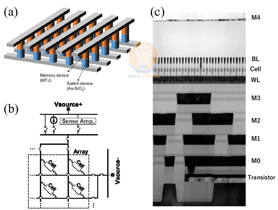
磁隧道结 RAM,使用磁机制而非电机制。来源:SK 海力士
At IEDM 2022, SK Hynix and Kioxia showed off a 1-selector MTJ cell with a 45nm pitch and 20nm critical dimension. Together, they achieved the highest MRAM density to date of 0.49 Gb/mm2, greater than Micron’s D1β DRAM which has a density of 0.435 Gb/mm2. The cell even features a 4F2 design. Their aim is to productize in discrete packages as an alternative to DRAM.
在 IEDM 2022 上,SK 海力士和 Kioxia 展示了一种具有 45nm 间距和 20nm 关键尺寸的 1 选择器 MTJ 单元。他们共同实现了迄今为止最高的 MRAM 密度为 0.49 Gb/mm²,超过了美光的 D1β DRAM,其密度为 0.435 Gb/mm²。该单元甚至采用了 4F2 设计。他们的目标是将其产品化为离散封装,作为 DRAM 的替代品。
At present none of the alternative memories are well placed to challenge DRAM. Some have larger or slower cells. Some have more expensive processes. Most have limited endurance. Some have low yield. In practice, the products shipping for magnetic or phase change memories are sized in MB not GB. This could change, there is a lot of money at stake and a winning combination may exist in stealth, but there is a lot of work on both devices and on scale of production to be done.
目前,没有任何替代存储器能够有效挑战 DRAM。有些具有更大或更慢的单元,有些则有更昂贵的工艺,大多数具有有限的耐用性,有些则产量低。在实际应用中,出货的磁性或相变存储器产品的容量以 MB 而非 GB 计。这种情况可能会改变,因为有大量资金在其中,可能存在一种隐秘的获胜组合,但在设备和生产规模方面还有很多工作要做。
Compute In Memory 在内存中计算
DRAM has been hamstrung from the beginning by its architecture. It is a simple state machine without any control logic, which helps keep the cost low, but means it depends upon the host (CPU) to control it.
DRAM 从一开始就受到其架构的限制。它是一个简单的状态机,没有任何控制逻辑,这有助于降低成本,但意味着它依赖于主机(CPU)来控制。
This paradigm is firmly entrenched: modern DRAM fabrication processes are so heavily optimized and specialized that they cannot realistically produce control logic. Industry group JEDEC (Joint Electron Devices Engineering Council) also enforces minimal intrusions from logic when developing new standards.
这一范式已深深扎根:现代 DRAM 制造工艺经过高度优化和专业化,实际上无法生产控制逻辑。行业组织 JEDEC(联合电子器件工程委员会)在制定新标准时也严格限制逻辑的干预。
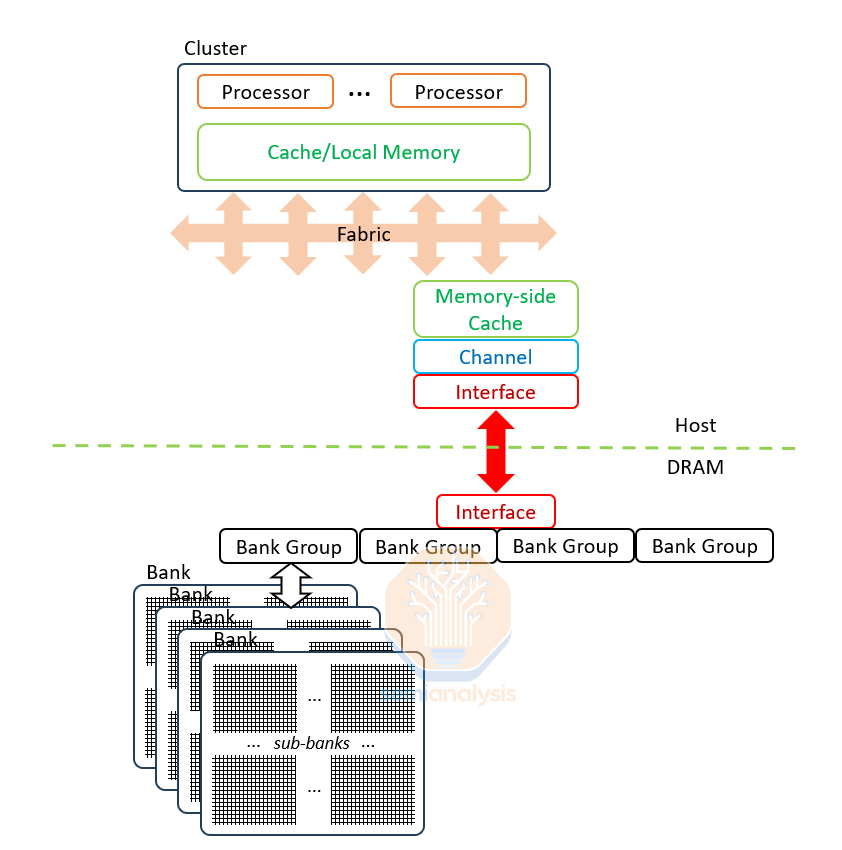
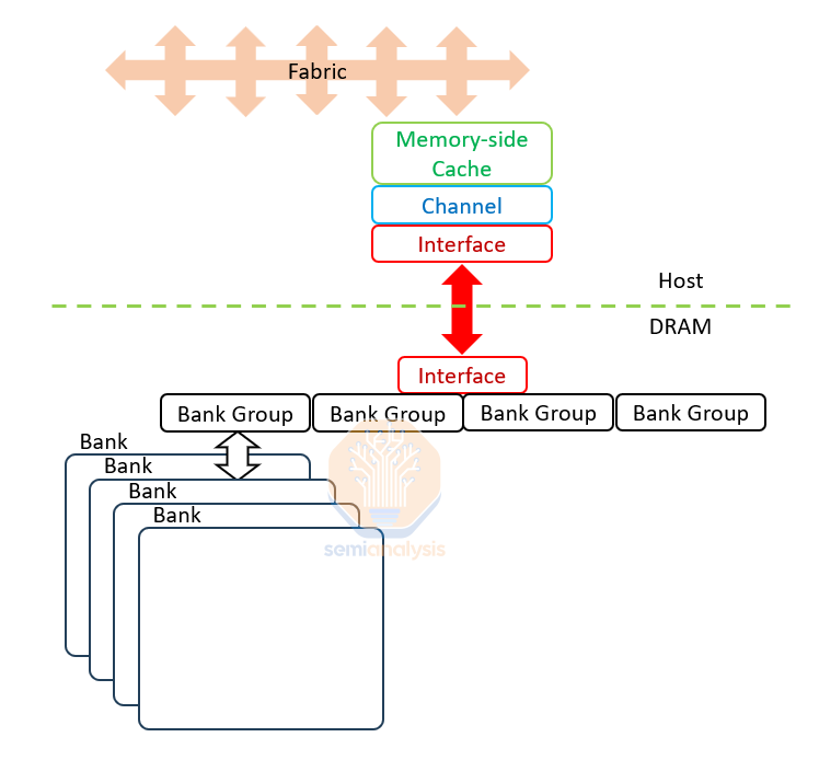
“傻瓜”DRAM:控制逻辑与内存分开,因此命令必须通过一个缓慢、低效的接口。来源:SemiAnalysis
The DRAM chip is totally dependent on the host: all commands are funneled through one shared interface for multiple banks in the memory, on behalf of multiple threads in the host. Each command requires 4 or more steps to be issued with precise timing to keep the DRAM functioning correctly. The DRAM chips don't even have the logic to avoid conflicts.
DRAM 芯片完全依赖于主机:所有命令通过一个共享接口传递给内存中的多个存储银行,代表主机中的多个线程。每个命令需要 4 个或更多步骤以精确的时序发出,以保持 DRAM 正常工作。DRAM 芯片甚至没有避免冲突的逻辑。
This is exacerbated by using an ancient half-duplex interface: a DRAM chip can read or write data but not both concurrently. The host has an exact model of the DRAM and must predict if the interface should be set to read or write for every clock cycle. Commands and data are sent on separate wires, which reduces timing complexity but increases the wire counts and “beach front” crowding on the GPU or CPU. Overall, the memory interface has dropped an order of magnitude below the bit rates, beach density, and efficiency of alternative PHYs used by logic chips.
这通过使用一种古老的半双工接口而加剧:DRAM 芯片可以读取或写入数据,但不能同时进行。主机对 DRAM 有一个精确的模型,必须预测在每个时钟周期中接口应该设置为读取还是写入。命令和数据在不同的线路上发送,这减少了时序复杂性,但增加了线路数量和 GPU 或 CPU 上的“海滩前沿”拥挤程度。总体而言,内存接口的性能已降至逻辑芯片所使用的替代物理层的比特率、海滩密度和效率的一个数量级以下。
The upshot of these disadvantages is that DDR5 DIMMs, the most common on servers, expend more than 99% of read or write energy in the host controller and interface. Other variants are slightly better – HBM energy use is roughly 95% interface, 5% memory cell read/write – but still nowhere near the full potential of DRAM.
这些缺点的结果是,DDR5 DIMM(服务器上最常见的内存)在主控和接口中消耗了超过 99%的读写能量。其他变种稍微好一些——HBM 的能量使用大约是 95%用于接口,5%用于内存单元的读写——但仍然远未达到 DRAM 的全部潜力。
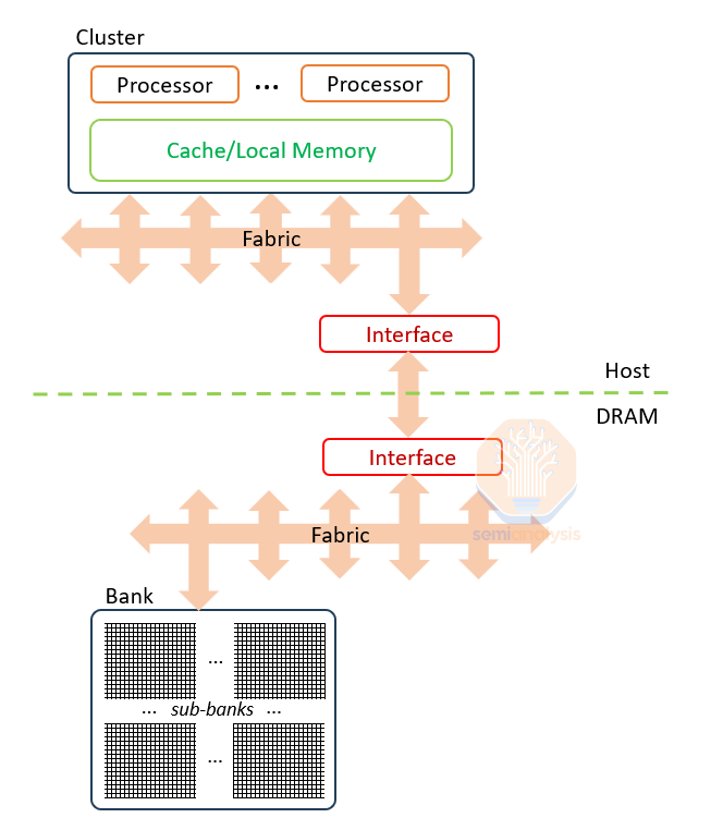
Functionality is simply in the wrong place. Naturally, the solution is to move it to the correct one: the control logic should be on-chip with the memory. This is Compute in Memory (CIM).
功能显然放错了地方。自然,解决方案是将其移动到正确的位置:控制逻辑应该与内存集成在芯片上。这就是内存计算(CIM)。
Compute in Memory: Unleash the Banks
在内存中计算:释放银行
DRAM banks have incredible performance potential that goes almost completely to waste because of interfaces.
DRAM 银行具有令人难以置信的性能潜力,但由于接口的原因,这种潜力几乎完全被浪费。
Banks are the basic unit of DRAM construction. They comprise 8 sub-banks each with 64Mb (8k rows by 8k bits) of memory. The bank activates and refreshes 1 row of 8k bits at once but transfers just 256 of them in or out in any I/O operation. This limitation is due to external connections from sense amplifiers: while the row is supported by 8k sense amplifiers, only 1 in 32 sense amplifiers (256) are connected out of the sub-bank, meaning read or write operation are limited to 256 bits
银行是 DRAM 构建的基本单元。它们由 8 个子银行组成,每个子银行具有 64Mb(8k 行×8k 位)的内存。银行一次激活和刷新 1 行 8k 位,但在任何 I/O 操作中仅传输 256 位。这个限制是由于来自传感放大器的外部连接:虽然该行由 8k 个传感放大器支持,但只有 32 个传感放大器中的 1 个(256)连接到子银行外,这意味着读或写操作限制为 256 位。
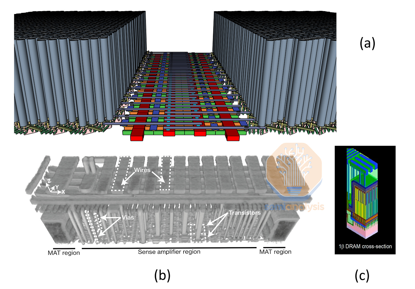
(a) 高密度的高电容器垫限制了对感应放大器的访问。来源:SemiAnalysis。 (b) 对 DDR4 DRAM 的感应放大器区域进行的聚焦离子束[FIB]拆解。来源:Marazzi 等人。“HiFi-DRAM:通过 IC 成像揭示感应放大器来推动高保真 DRAM 研究”,ISCA 2024 (c) 1β DRAM 中垫区边缘的图形。来源:美光
The sense amps are in a canyon surrounded by tall capacitors. In the FIB teardown above from ETH Zurich you can see there is wiring at higher levels which needs tall vias stretching down to make contacts to the sense amps.
感应放大器位于一个被高电容器环绕的峡谷中。在上面的 ETH 苏黎世的 FIB 拆解中,可以看到在更高的层级有布线,这需要高通孔向下延伸以与感应放大器接触。
Even with this limited interface, 1 in 32 accessible at any one time, the peak read/write capacity of a bank is roughly 256Gb/s, with an average closer to 128 Gb/s as at least 50% of time is used in switching to a new active row. With 32 banks per 16Gb chip the full potential of one chip is 4TB/s.
即使在这种有限的接口下,任何时候可访问的数量为 32 个中的 1 个,银行的峰值读写能力大约为 256Gb/s,平均接近 128Gb/s,因为至少 50%的时间用于切换到新的活动行。每个 16Gb 芯片有 32 个银行,一个芯片的全部潜力为 4TB/s。
Further up the hierarchy, banks are connected in bank groups, which in turn connect to the interface out of the DRAM chip. In HBM, each die has 256 data lines with a peak throughput of 256 GB/s per die. This bottleneck can utilize only 1/16th of the underlying potential of the banks.
在层级的更高处,银行通过银行组相互连接,这些银行组又连接到 DRAM 芯片的接口。在 HBM 中,每个芯片有 256 条数据线,每个芯片的峰值吞吐量为 256 GB/s。这个瓶颈只能利用银行潜在能力的 1/16。
To add insult to injury, 2pJ of energy are needed to transfer a single bit out of the chip, 20x more than it took to move it in or out of the cell. Most of that happens at the two interfaces on each end of the DQ (Data Question-mark, a data line which is used for both read and write) wires, and in the controller logic on the host.
为了雪上加霜,转移一个比特出芯片需要 2pJ 的能量,这比将其进出单元所需的能量多 20 倍。大部分能量消耗发生在 DQ(数据问号,一种用于读写的数据线)线两端的两个接口,以及主机上的控制逻辑中。
With such a wasteful architecture, it’s inevitable that efforts will be made to access more of the potential performance.
在如此浪费的架构下,必然会努力去挖掘更多的潜在性能。
Compute in Memory: The Full Potential of DRAM
在内存中计算:DRAM 的全部潜力
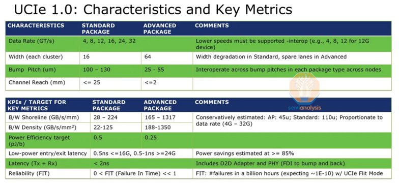
Even simple theoretical examples show there is massive potential on offer here. Implementing the UCIe (Universal Chiplet Interconnect) standard would allow for 11 Tbps throughput per mm of edge – nearly 12x better than HBM3E. Energy per bit would go down by an order of magnitude from 2pJ to 0.25pJ. And UCIe is not even the latest solution… Eliyan’s proprietary Nulink standard, to take just one example, claims even greater improvements.
即使是简单的理论示例也显示出这里有巨大的潜力。实施 UCIe(通用芯片互连)标准将允许每毫米边缘达到 11 Tbps 的吞吐量——几乎是 HBM3E 的 12 倍。每比特的能耗将从 2pJ 降低一个数量级至 0.25pJ。而 UCIe 甚至不是最新的解决方案……以 Eliyan 的专有 Nulink 标准为例,声称有更大的改进。
The caveat here is that if the host fabric is extended across the interface, then a subset of the fabric command set must be handled on the DRAM side. Each bank would need to implement the state machine (pre-charge, address select, activate, read/write, close, etc.) locally. This requires (relatively) complex logic fabricated on-chip with the DRAM.
这里的警告是,如果主机结构跨越接口扩展,则必须在 DRAM 端处理结构命令集的一个子集。每个存储银行需要在本地实现状态机(预充电、地址选择、激活、读/写、关闭等)。这需要在 DRAM 上芯片内制造(相对)复杂的逻辑。
Compute in Memory: Path Forward & Possible Winners
内存计算:前进路径与可能的赢家
Adding logic to a DRAM chip is, of course, no simple task. The good news is that HBM includes a CMOS base chip, and when 3D DRAM arrives there is a virtual certainty that good CMOS logic is bonded atop or underneath the memory stack. In other words, the architecture is amenable to including some compute within memory, and chipmakers will be incentivized to do so.
在 DRAM 芯片中添加逻辑当然不是一件简单的事情。好消息是,HBM 包括一个 CMOS 基础芯片,当 3D DRAM 到来时,几乎可以肯定在内存堆栈的顶部或底部会结合良好的 CMOS 逻辑。换句话说,这种架构适合在内存中包含一些计算,芯片制造商将有动力这样做。
There is low hanging fruit here: consider what could be done if HBM adopted the GDDR7 rate of 32Gbps per data wire. GDDR7 demonstrates that fast enough transistors can be made on the DRAM chips, and the vertical distance through the TSVs to the base stack is under 1mm which should keep energy per bit in the 0.25pJ/bit range. It begs the question: why would JEDEC not lean into an improved standard here?
这里有一些简单的机会:考虑如果 HBM 采用每条数据线 32Gbps 的 GDDR7 速率可以做些什么。GDDR7 表明可以在 DRAM 芯片上制造足够快的晶体管,并且通过 TSV 到基堆的垂直距离低于 1mm,这应该将每比特的能量保持在 0.25pJ/bit 范围内。这引发了一个问题:为什么 JEDEC 不在这里推动一个改进的标准?
The external interfaces on the base chip could be substantially upgraded to modern designs offering more than a terabyte/sec per mm of edge, at fractional pJ energy per bit. Someone is going to win big in the IP wars. While it’s possible that JEDEC will adopt one choice as standard, more likely it will be done by faster-moving memory / GPU-vendor pairs, as JEDEC usually takes years.
基础芯片上的外部接口可以大幅升级为现代设计,提供每毫米边缘超过一太字节/秒的速度,能耗为每比特几分皮焦耳。某些公司将在知识产权战争中获得巨大的胜利。虽然 JEDEC 可能会将某个选择作为标准,但更可能的是由快速发展的内存/GPU 供应商组合来完成,因为 JEDEC 通常需要数年时间。
We already see real change possible in HBM4 with the acceptance of 3rd party base chips, which is bound to unleash experiments. We will likely see offloaded channel control, pure fabric extension on the interconnect, reduced energy per bit over centimeters of distance, and daisy chaining to other rows of HBM further from the host, or to 2nd tier memory like banks of LPDDR.
我们已经看到在 HBM4 中接受第三方基础芯片可能带来的真正变化,这必将释放实验的潜力。我们可能会看到卸载的通道控制、在互连上的纯织物扩展、在厘米距离上的每比特能耗降低,以及与离主机更远的其他 HBM 行或二级内存(如 LPDDR 银行)的串联。
In this way designs can sidestep the power limits of trying to do compute inside the memory stack and instead use a modernized interface on the base chip to allow neighboring chips the bandwidth and low energy per bit for compute as-if in memory.
通过这种方式,设计可以绕过在内存堆栈中进行计算的功率限制,而是使用基础芯片上的现代化接口,使相邻芯片能够以类似内存的方式提供带宽和每比特低能耗的计算。
Below we’ll cover the coming revolution in DRAM: 3D. This will mean a tectonic shift for the memory manufacturers and wafer fab equipment - we’ll discuss basics, how it’s manufactured, and likely winners (and losers).
下面我们将讨论即将到来的 DRAM 革命:3D。这将意味着内存制造商和晶圆制造设备的重大变革——我们将讨论基础知识、制造过程以及可能的赢家(和输家)。
3D DRAM: Basics 3D DRAM:基础知识
Unlike emerging memory architectures, 3D DRAM is based on a well-known foundation: the 1T1C Dennard cell. It builds upon decades of research and practical experience with conventional DRAM, the one major change being fabrication technique. It also happens to be generally compatible with CIM architectures. In other words, it appears to be the lowest risk long-term option.
与新兴内存架构不同,3D DRAM 基于一个众所周知的基础:1T1C Dennard 单元。它建立在数十年的传统 DRAM 研究和实践经验之上,唯一的重大变化是制造技术。它通常与 CIM 架构兼容。换句话说,它似乎是风险最低的长期选择。
As discussed earlier, current DRAM cells use 6F2 designs with 4F2 coming soon. In general these architectures seek to reduce the horizontal footprint in exchange for increasing vertical footprint. They may offer speed improvements but, since capacitor packing is not directly affected, overall density may not change by much.
如前所述,目前的 DRAM 单元使用 6F2 设计,4F2 设计即将推出。一般来说,这些架构旨在减少水平占地面积,以换取增加垂直占地面积。它们可能提供速度提升,但由于电容器的封装不受直接影响,整体密度可能不会有太大变化。
3D DRAM takes an entirely different tack. Instead of squeezing the last few atoms of horizontal shrink at great difficulty, one can rotate the capacitors and stack them atop each other. Scaling is achieved not via shrink but by stacking more and more layers in the device.
3D DRAM 采取了完全不同的方法。与其费力地挤压最后几原子的水平缩小,不如旋转电容器并将其堆叠在一起。缩放不是通过缩小实现的,而是通过在设备中堆叠越来越多的层来实现的。
NAND went through this transition (rotation to vertical) a decade ago and has gone from 32 layers in the first commercial products, now to 1000 within sight. With the caveat that DRAM’s 1T1C architecture is significantly more complex than NAND, the guiding principle is to lay down featureless, cheap layers and use clever top-down etching along with chemistry to form all the transistors and capacitors in parallel.
NAND 在十年前经历了这一转变(旋转到垂直),从首批商业产品的 32 层,现在已接近 1000 层。需要注意的是,DRAM 的 1T1C 架构比 NAND 复杂得多,但指导原则是铺设无特征、廉价的层,并利用巧妙的自上而下蚀刻和化学方法并行形成所有晶体管和电容器。
CMOS for sense amps and periphery will be integrated above or below the memory cell stack. This might come on top by hybrid bonding, or on bottom by flip and thinning to use the back side for a fresh silicon surface with vias reaching down to the vertical lines. The circuitry in either version is no longer limited to slow transistors and, with more bits per chip, there will be incentive to add better interface functionality and efficiency. These chips will likely have a whole new class of interface.
CMOS 用于传感放大器和外围电路将集成在存储单元堆栈的上方或下方。这可能通过混合键合在顶部实现,或通过翻转和减薄在底部实现,以利用背面获得新的硅表面,并通过通孔连接到垂直线路。无论哪种版本,电路不再局限于慢速晶体管,随着每个芯片的位数增加,将有动力增加更好的接口功能和效率。这些芯片可能会拥有全新类别的接口。
3D DRAM: Underdogs 3D DRAM:黑马
3D is a disruptive shift in how DRAM is produced, and it’s not guaranteed the incumbents will remain in their positions atop the market. The smaller players, while at a disadvantage in terms of raw R&D firepower and ability to quickly scale production, are not completely out of the game when it comes to 3D DRAM.
3D 是 DRAM 生产方式的颠覆性转变,现有企业在市场上的地位并不一定能够保持。虽然小型企业在研发实力和快速扩大生产能力方面处于劣势,但在 3D DRAM 领域并非完全被淘汰。
Macronix demonstrated 3T0C (3 transistor, 0 capacitor, a gain cell like the 1973 Intel device) DRAM at IEDM 2022, with a pathway to 3D stacking and a GAA architecture. The cell size of the stacked version would be 21F2, so only 4 layers would be needed to surpass current density, assuming feature sizes remain the same.
美光在 2022 年 IEDM 上展示了 3T0C(3 个晶体管,0 个电容,类似于 1973 年英特尔设备的增益单元)DRAM,具有 3D 堆叠和 GAA 架构的路径。堆叠版本的单元大小为 21F2,因此只需 4 层即可超过当前密度,假设特征尺寸保持不变。
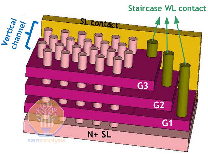
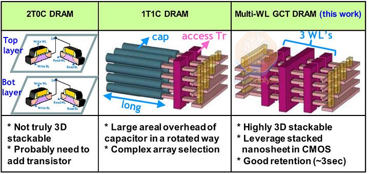
来源: Macronix IEDM 2022
There are various other concepts published by smaller manufacturers. Keep in mind the massive capex that would be needed to scale production and the minefield of existing IP, most of it owned by the largest memory manufacturers. It remains to be seen if any of the small players can make a disruptive leap to production.
还有许多较小制造商发布的其他概念。请记住,扩大生产所需的巨额资本支出以及现有知识产权的复杂局面,其中大部分由最大的内存制造商拥有。尚不清楚是否有任何小型参与者能够实现生产上的颠覆性突破。
3D DRAM: the Big 3
3D DRAM:三大巨头
Samsung recently made news with their roadmap (reprinted above in the short-term scaling section) showing 3D DRAM at Memcon 2024. This is the first time we are seeing it officially on roadmaps – a strong signal that the technology is being pushed from lab towards real production.
三星最近在新闻中发布了他们的路线图(在短期扩展部分上方重印),显示了 2024 年 Memcon 上的 3D DRAM。这是我们第一次在路线图上正式看到它——这是一个强烈的信号,表明该技术正从实验室向实际生产推进。
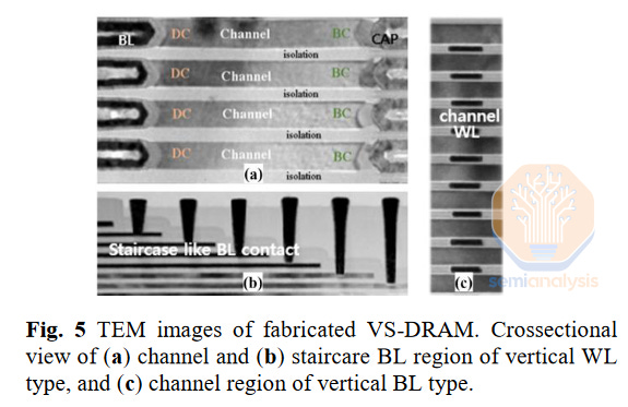
Samsung’s name for 3D is “VS-DRAM” for “vertically stacked.” Their published work is very early given that both vertical wordline and vertical bitline schemes are shown. Actual images are limited in detail although electrical characterization was done on a vertical wordline chip, so at least they can produce functioning devices. These results, to be fair, are a year old but still point to early development rather than production-ready.
三星对 3D 的名称是“VS-DRAM”,意为“垂直堆叠”。他们发布的工作非常早,因为展示了垂直字线和垂直位线方案。实际图像细节有限,尽管在垂直字线芯片上进行了电气特性测试,因此至少他们可以生产出功能设备。公平地说,这些结果已有一年,但仍然指向早期开发而非生产就绪。
SK Hynix is the first to put a stake in the ground at the 0a node. They came in guns blazing at VLSI 2024 with detailed results on a 5-layer vertical BL integration. After the upcoming 1c and 1d nodes, they say the process integration and scaling challenges will justify introducing 3D for 0a. That puts the transition roughly 5 years out.
SK 海力士是首个在 0a 节点上立足的公司。他们在 2024 年 VLSI 大会上以详细的 5 层垂直 BL 集成结果强势登场。在即将到来的 1c 和 1d 节点之后,他们表示,工艺集成和缩放挑战将证明在 0a 节点引入 3D 的必要性。这使得过渡大约在 5 年后。
They argue that vertical bitline is clearly the correct architecture, as it affords more sensing margin. A fully integrated device was shown – including the memory array and peripheral circuitry connected via hybrid bonding.
他们认为垂直位线显然是正确的架构,因为它提供了更大的感应余量。展示了一个完全集成的设备——包括通过混合键合连接的存储阵列和外围电路。
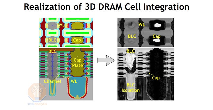
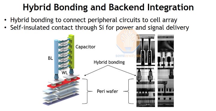
SK 海力士首次展示 5 层 3D DRAM。来源:SK 海力士 VLSI 2024:
They note that more work is required here. Expect the details of the architecture and integration scheme to evolve before high volume production. While a complete chip with a 5-layer stack is impressive at this juncture, close to 10x more layers will be needed for a viable high volume manufacturing process.
他们指出这里需要更多的工作。预计架构和集成方案的细节将在大规模生产之前不断演变。虽然在此阶段,具有 5 层堆叠的完整芯片令人印象深刻,但要实现可行的大规模制造过程,可能需要接近 10 倍的层数。
Micron of course is subject to similar scaling challenges for 2D and has come to the same conclusion that 3D DRAM is needed, but has shown essentially no public work to that effect. There are signs of R&D work – for example, a keynote at IITC 2024 mentioned the difficulty of producing high quality Si/SiGe layer stacks for 3D DRAM – but little else. At IEDM 2023, Micron’s Dr. Tran noted that “patterning cost is exploding…” which naturally leads down the 3D path to reduce that cost. Possibly they see a longer timeline; their 1β node achieves industry-leading density without EUV, so they may be able to squeeze a few more nodes below 10nm class before going 3D.
美光当然面临类似的 2D 缩放挑战,并得出了需要 3D DRAM 的相同结论,但实际上几乎没有公开的相关工作。有研发工作的迹象——例如,2024 年 IITC 的主题演讲提到生产高质量 Si/SiGe 层堆叠用于 3D DRAM 的困难——但其他方面很少。在 2023 年 IEDM 上,美光的 Tran 博士指出“图案化成本正在飙升……”,这自然引导我们走向 3D 路径以降低该成本。可能他们看到更长的时间线;他们的 1β节点在没有 EUV 的情况下实现了行业领先的密度,因此在转向 3D 之前,他们可能能够在 10nm 以下再挤出几个节点。
3D DRAM: Fabrication and Equipment
3D DRAM:制造与设备
Generally, the transition from horizontal to vertical scaling means a shift in the equipment enabling it. In all 3 major applications – NAND, DRAM, logic – lithography is the primary driver of horizontal scaling. It’s intuitive: to manufacture smaller devices, you need to print smaller features. Vertical scaling in 3D DRAM is instead driven by materials processing. Horizontal dimensions that drive lithography requirements stay mostly unchanged, and the challenges shift to deposition, etch, and similar: how do you etch a hole with 100:1 aspect ratio? How do you deposit a high-quality film 1nm thick on the underside of a Si channel without line of sight? And so on…
通常,从横向扩展到纵向扩展意味着支持这种转变的设备发生了变化。在所有三大主要应用中——NAND、DRAM、逻辑——光刻是横向扩展的主要驱动因素。这是直观的:要制造更小的设备,您需要打印更小的特征。3D DRAM 中的纵向扩展则是由材料处理驱动的。驱动光刻要求的横向尺寸基本保持不变,挑战转向沉积、刻蚀等方面:如何刻蚀一个长宽比为 100:1 的孔?如何在没有视线的情况下在硅通道的底面沉积一层 1nm 厚的高质量薄膜?等等……
2D NAND historically drove the most aggressive lithography pitch scaling as it required the most aggressive horizontal shrink out of the 3 major leading-edge applications (NAND, DRAM, logic). Density increases were primarily attained via horizontal shrink of the memory cell. The switch to 3D NAND & layer scaling decoupled lithography scaling from the roadmap, as density scaling is achieved by simply adding more vertical layers while the memory cell stays the same size.
2D NAND 历史上推动了最激进的光刻间距缩放,因为它在三大领先应用(NAND、DRAM、逻辑)中需要最激进的水平缩小。密度的增加主要是通过内存单元的水平缩小来实现的。转向 3D NAND 和层缩放使光刻缩放与路线图解耦,因为密度缩放仅通过添加更多的垂直层来实现,而内存单元的大小保持不变。
The big opportunities in 3D NAND are for the materials players – for example, in cryo tools for high aspect ratio etch.
3D NAND 的大机会在于材料供应商——例如,用于高纵横比刻蚀的低温工具。
Expect a similar dynamic for DRAM’s switch to 3D.
预计 DRAM 向 3D 的转换将呈现类似的动态。
DRAM lithography layer counts have also grown quite slowly through the 2y and 10nm generations. But layers have gradually moved to more and more expensive tools as horizontal scaling continues – low-NA EUV tools now make sense for a few critical layers, and if not for the transition to 3D, high-NA would be on the roadmap.
DRAM 光刻层数在 2y 和 10nm 代中也增长得相当缓慢。但随着水平缩放的持续,层数逐渐转向越来越昂贵的工具——低 NA EUV 工具现在对一些关键层来说是合理的,如果不是为了向 3D 过渡,高 NA 将会在路线图上。
It’s worth going into a little detail on the process flows for conventional vs. 3D. Not only because it’s interesting but also to prove out the theory on shift from lithography to etch and deposition. This is a big change in value capture for equipment manufacturers, as those who enable scaling can generally command higher premiums.
值得详细讨论传统工艺与 3D 工艺的流程。这不仅因为它有趣,还为了证明从光刻转向蚀刻和沉积的理论。这对设备制造商来说是一个价值捕获的重大变化,因为那些能够实现规模化的公司通常可以收取更高的溢价。
Conventional DRAM has an unintuitive structure as it utilizes a number of clever tricks to increase density. Current flow follows a “U” shape from bitline, down around a saddle-shaped channel surrounded by a gate, and back up into the storage node capacitor.
传统的 DRAM 具有一种不直观的结构,因为它利用了许多巧妙的技巧来增加密度。电流沿着“U”形从位线流出,绕过一个被栅极包围的鞍形通道,然后回到存储节点电容。
Conventional DRAM process flow. Source: SemiAnalysis
常规 DRAM 工艺流程。来源:SemiAnalysis
The manufacturing scheme naturally must flow from bottom-up:
制造方案自然必须自下而上进行:
Active Silicon regions with gates and wordlines to control them are formed first, “buried” beneath the rest of the device. This reduces parasitic capacitance from the interaction between the wordline and bitline. Next contacts are built above the active regions, these connect to the sources & drains for the access transistor. Bitlines are made in a line/space pattern forming continuous rows connecting to only half of the contacts. Finally storage node capacitors are built atop the other half of the contacts.
首先形成带有栅极和字线以控制它们的活跃硅区域,这些区域“埋”在设备的其余部分之下。这减少了字线和位线之间相互作用产生的寄生电容。接下来,在活跃区域上方构建接触点,这些接触点连接到访问晶体管的源极和漏极。位线以线/间隔模式制造,形成连续的行,仅连接到一半的接触点。最后,存储节点电容器建造在另一半接触点的顶部。
For a 10nm-class DRAM, the pitch of these features is at most 48nm– near or below even the most aggressive gate pitches for leading logic processes. This demands lithography tools with exceptional overlay performance, especially when employing multi-patterning schemes. In other words it demands the most expensive lithography tools. Most importantly, the key features are placed and defined via lithography.
对于 10nm 级 DRAM,这些特征的间距最多为 48nm——接近或低于领先逻辑工艺中最激进的栅极间距。这要求光刻工具具有卓越的叠加性能,特别是在采用多图案方案时。换句话说,这要求使用最昂贵的光刻工具。最重要的是,关键特征是通过光刻进行放置和定义的。
3D DRAM in contrast to conventional is relatively simple and intuitive (note that we will describe a vertical BL scheme as that seems to be the most promising). A vertical bitline runs from top to bottom. Horizontal channels connect out from the bitline with gates and wordline on top and bottom of the channel. The other end of the channel terminates at a capacitor, which lies flat and stacked atop others in an array.
3D DRAM 与传统 DRAM 相比相对简单直观(请注意,我们将描述一种垂直位线方案,因为这似乎是最有前景的)。垂直位线从顶部到底部延伸。水平通道从位线连接出来,通道的顶部和底部有栅极和字线。通道的另一端终止于一个电容器,该电容器平放并堆叠在阵列中的其他电容器上。
Current flow between the bitline and capacitors is controlled by the gate/wordline between them.
当前比特线与电容器之间的电流由它们之间的栅极/字线控制。
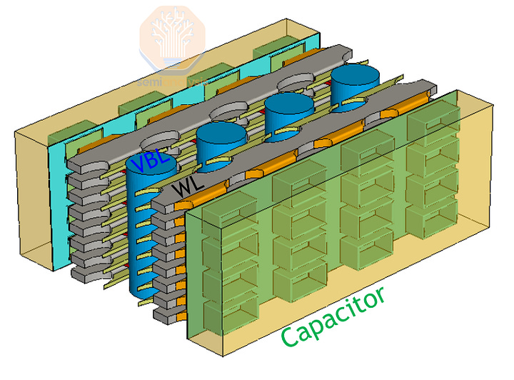
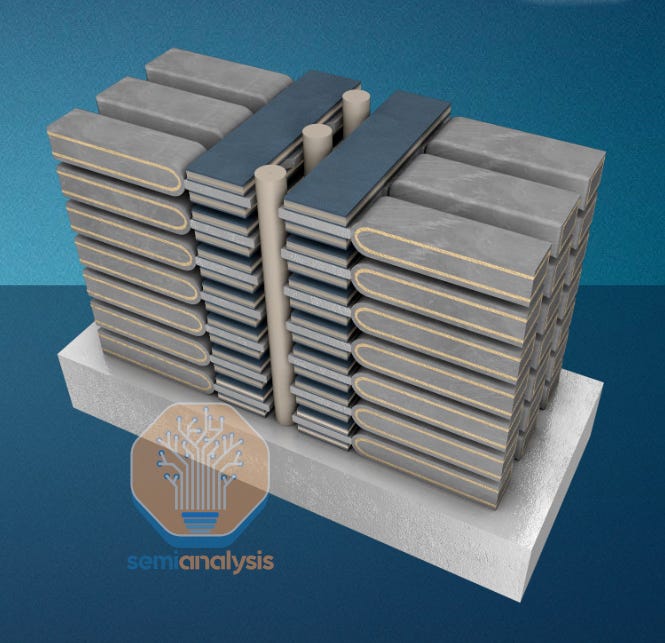
3D DRAM 具有垂直位线(VBL)、水平字线(WL)和水平电容阵列。在第二张图中,垂直位线显示为带有浅蓝色通道的圆柱体,深蓝色字线位于这些通道的上下方。来源:SK 海力士 VLSI 2024,应用材料公司
While we are simplifying some steps for clarity and because the process is still being developed, a representative process flow is as follows:
虽然我们为了清晰而简化了一些步骤,并且该过程仍在开发中,但代表性的流程如下:
A theoretical 3D DRAM manufacturing flow. Source: SemiAnalysis
理论上的 3D DRAM 制造流程。来源:SemiAnalysis
Fabrication begins with a stack of alternating Si/SiGe layers, similar to the beginning of a gate all around transistor. Isolation pillars are formed by etching holes and filling with dielectric. These insulate the bitlines from each other and support the Si layers through the rest of the fabrication process. Another set of holes that will eventually form the vertical bitlines and capacitor arrays are cut out in a grid that avoids the isolation pillars.
制造从交替的 Si/SiGe 层堆叠开始,类似于全环栅晶体管的开始。通过蚀刻孔并填充介电材料形成隔离柱。这些隔离柱将位线相互绝缘,并在整个制造过程中支撑 Si 层。另一组孔最终将形成垂直位线和电容阵列,以避免隔离柱的网格中切割。
Through these open holes the sacrificial SiGe is etched out, leaving horizontal Si layers suspended by the isolation pillars. These Si layers will eventually serve as the channels connecting BL to capacitor. A nitride layer is deposited to “wrap” around the channels and isolation material is also deposited in the remaining space as insulation against current leakage to adjacent channels.
通过这些开放的孔,牺牲的 SiGe 被蚀刻掉,留下由隔离柱悬挂的水平 Si 层。这些 Si 层最终将作为连接 BL 到电容器的通道。氮化物层被沉积以“包裹”通道,隔离材料也在剩余空间中沉积,以防止电流泄漏到相邻通道。
The capacitor holes are filled with a dummy material to plug them while bitlines are left open. Through these open holes, the nitride surrounding the channel can be etched back slightly and replaced with gates + a metal wordline.
电容器孔被填充了假材料以进行封堵,同时位线保持开放。通过这些开放的孔,围绕通道的氮化物可以稍微蚀刻回去,并用栅极和金属字线替换。
Now the bitlines are formed by filling the open holes with metal. Last the capacitors are built by removing dummy fill from the capacitor holes and replacing with capacitive bulk material.
现在,位线通过用金属填充开放孔形成。最后,通过从电容孔中去除虚拟填充并用电容体材料替换来构建电容器。
While we omit some key details such as how the contacts from bitline to channel and channel to capacitor are engineered, the overall theme should be clear: there are relatively few patterning steps and many difficult etch/deposition steps.
虽然我们省略了一些关键细节,例如从比特线到通道以及从通道到电容器的接触是如何设计的,但整体主题应该很清楚:图案化步骤相对较少,而困难的刻蚀/沉积步骤则很多。
Current state-of-the-art processes require high aspect ratio (10:1 – 100:1) hole etches. The 3D DRAM process is significantly harder: etch and deposition must access the bottom of high aspect ratio holes and then laterally, without line-of-sight, into a high aspect ratio channel. It’s going to be very challenging to do this, most likely with a combination of cryo etch for the vertical followed by wet etch for the horizontal.
当前最先进的工艺需要高纵横比(10:1 – 100:1)孔蚀刻。3D DRAM 工艺则更为复杂:蚀刻和沉积必须能够到达高纵横比孔的底部,然后在没有视线的情况下横向进入高纵横比通道。这将非常具有挑战性,最有可能采用垂直的低温蚀刻与水平的湿蚀刻相结合。
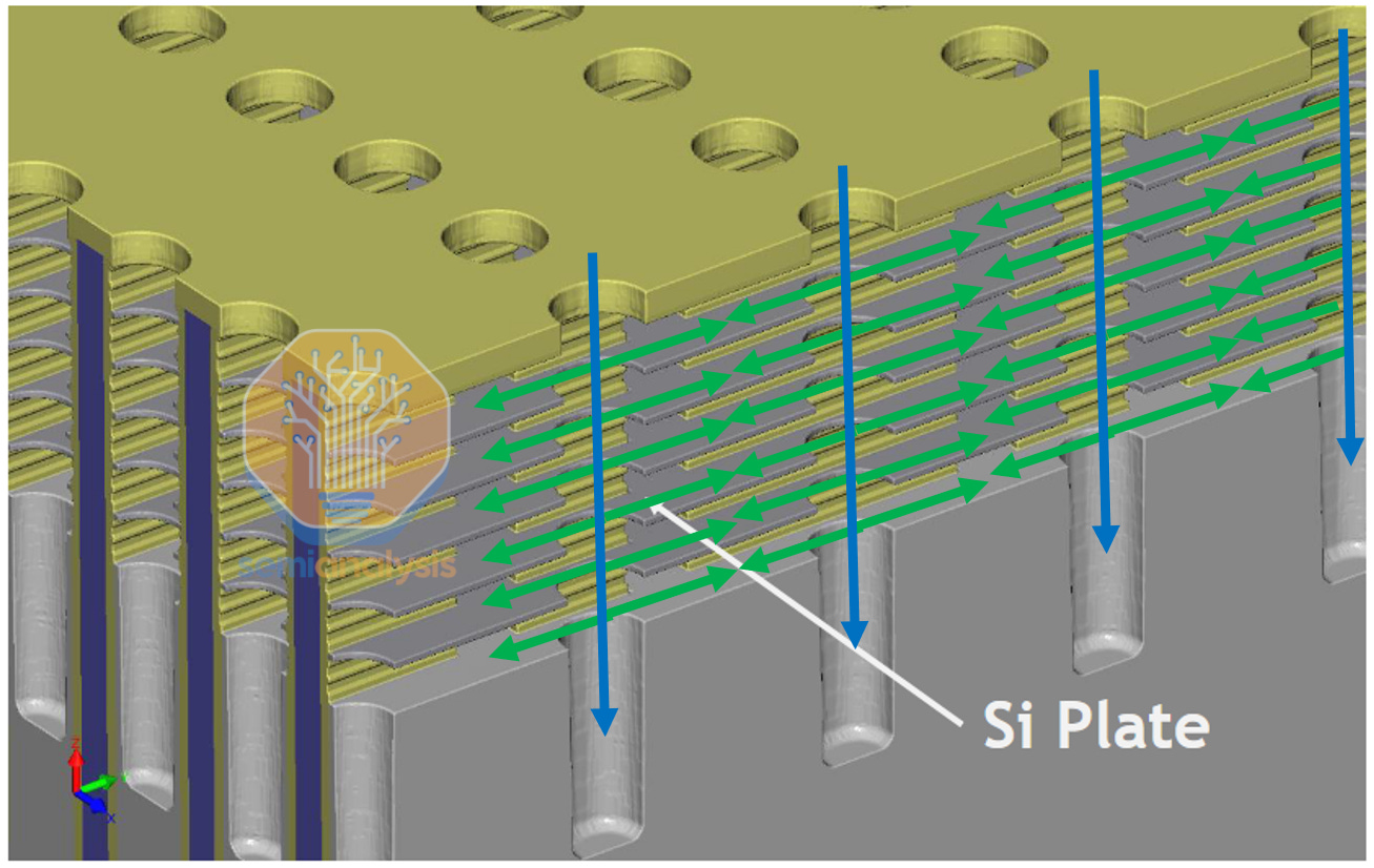
非视距、高纵横比蚀刻用于 3D DRAM。来源:SK 海力士,SemiAnalysis
In short, expect lithography intensity to reduce from the 25% range for conventional DRAM to roughly half that for 3D DRAM, with that share shifting to etch and deposition tools. While most vendors are publicly saying ~2030 for 3D DRAM, the increased incentives from AI demand may accelerate that timeline.
简而言之,预计传统 DRAM 的光刻强度将从 25%左右降低到 3D DRAM 的约一半,而这一份额将转移到刻蚀和沉积工具上。虽然大多数供应商公开表示 3D DRAM 将在 2030 年左右推出,但来自 AI 需求的增加激励可能会加速这一时间表。


