
The silicon chip, or integrated circuit (IC), is one of humankind’s most magnificent, complex, and transformative creations.
矽芯片或集成電路(IC)是人類最宏偉,最複雜和變革性的創造之一。
The IC itself is a silicon sandwich made up of many transistors (little switches) wired together into electrical circuits. Since Robert Noyce and Jack Kilby’s coinvention of the IC in 1958-59, relentless improvements in transistor density have taken place. You could see this change in spacecraft, aviation, communications, and, most obviously for most of us, in the consumer products of their times. In the early days of ICs, for example, one of the earliest products was the basic four-function 1973 Sears/Bowmar handheld calculator. Sixty years later, the hot consumer product is a voice activated smartphone connected to the "world brain" of the internet—science fiction only a generation ago.
IC本身是由許多晶體管(小開關)組成的矽三明治,將它們一起連接到電路中。自從羅伯特·諾伊斯(Robert Noyce)和傑克·基爾比(Jack Kilby)在1958 - 59年對IC的匯總進行了貢獻以來,晶體管密度的不斷改善。您可以看到航天器,航空,通訊以及對我們大多數人的消費產品的這種變化。例如,在IC的早期,最早的產品之一是1973年的Sears/Bowmar手持計算器的基本四功能。六十年後,熱消費品是一種與互聯網“世界大腦”相連的聲音激活的智能手機 - 僅一代人就在一代小說中。
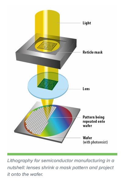
It took a long time to get there, but the progress was steady: since Fairchild Semiconductor chemical engineer Gordon Moore first wrote about ICs in 1965, roughly every 18–24 months the number of transistors on an integrated circuit has doubled. The basic process that has allowed this is photolithography, which, if you break it down into its Greek origins means “writing on stone with light.” Figure 1 below shows the general idea.
到達那里花了很長時間,但是進步卻穩定了:因為Fairchild半導體工程師戈登·摩爾(Gordon Moore)於1965年首次撰寫了有關ICS的文章,大約每18-24個月,綜合電路上的晶體管數量增加了一倍。允許這是光刻的基本過程,如果將其分解成希臘的起源,則意味著“用光寫在石頭上”。下圖1顯示了總體想法。
Source: https://bits-chips.nl/artikel/euv-for-dummies/
資料來源:https: //bits-chips.nl/artikel/euv-for-dummies/
Light (often ultraviolet) is blasted through a stencil with the patterns IC designers want burned into the chip. Special chemicals are applied before and after to allow this and the process is repeated until a sandwich, made up of many layers, has been built up and the IC is finished and ready for packaging.
光線(通常是紫外線)通過模板爆炸,圖案IC設計師希望將其燃燒成芯片。在允許之前和之後使用特殊的化學品,並重複該過程,直到由許多層組成的三明治已建立,並且IC已完成並準備好包裝。
Computer designer Gordon Bell once noted that getting the highest speed possible in computers—which rely entirely on ICs—is often about "plumbing and packaging." Since integrated circuits get hotter the faster they run, fast computers have to worry about keeping their chips cool. We can see this limitation echoed this in the observation that several of legendary supercomputer designer Seymour Cray’s patents were related to ways of keeping his world-beating computer systems cool. For Cray, who always pushed the limits of the possible, keeping the system from burning up was just as important as designing fast circuits.
計算機設計師戈登·貝爾(Gordon Bell)曾經指出,完全依靠IC的計算機中獲得最高速度,通常與“管道和包裝”有關。由於集成電路的運行速度越快,快速計算機必須擔心保持芯片涼爽。我們可以看到,這一局限性在觀察到的觀察結果中回應了這一點,即傳奇的超級計算機設計師西摩·克雷(Seymour Cray)的專利與保持世界娛樂計算機系統涼爽的方式有關。對於總是推動可能的限制的克雷來說,防止系統燃燒與設計快速電路一樣重要。
Cerebras, a well-funded Silicon Valley startup, has developed one of the most ingenious and technically elegant solutions to the problem of both "cramming" (to paraphrase Gordon Moore) more transistors onto a chip while keeping it cool. How far could things be pushed? The answer is astounding: on a huge, single square piece of silicon, about 8.5” on a side, the Cerebras Wafer-Scale Engine (WSE) has 2.6 trillion transistors, which make up 850,000 AI-optimized processing units. (Figure 2.) The size of a transistor in the WSE is 7 nanometers. Human DNA is 2.5 nanometers. There are more transistors—by far—in this one Cerebras chip than in all 100,000 computing objects combined in the Museum’s permanent collection.
Cerebras是一家資金良好的矽谷初創公司,它開發了一種最巧妙,技術優雅的解決方案之一,以解決“擠滿”(釋放戈登·摩爾(Gordon Moore))的問題,同時將更多的晶體管放到芯片上,同時保持其涼爽。事情可以推到多遠?答案令人震驚:在一塊巨大的單方面矽上,一側約8.5英寸,腦晶圓尺度發動機(WSE)具有2.6萬億晶體管,構成了850,000 AI-AI-PRISTISPISTIEM PROCESTING STISTORS。 (圖2.)WSE中晶體管的大小為7納米。人DNA為2.5納米。在這個小腦芯片中,有更多的晶體管比博物館永久收藏中的所有100,000個計算對像中的晶體管要多。
Figure 2. The Cerebras Wafer-Scale Engine
圖2。小腦晶圓尺度發動機
What’s clever about the WSE is that its design and manufacturing largely follow existing industry processes and methods. Their unique genius was in providing a state-of-the-art ecosystem for the WSE to live in—one which supplied it with power, cooling, and communications.
WSE的聰明是它的設計和製造在很大程度上遵循現有的行業流程和方法。他們獨特的天才是為WSE提供了一個最先進的生態系統,該系統為其提供了動力,冷卻和通信。
To pull this off Cerebras relies not on some exotic new method or technology but on existing semiconductor fabrication processes—just modifying them slightly. (The 8.5” on a side footprint, for example, is what’s left when you take a standard 300 mm wafer and cut it into a square).
要脫掉腦,腦部不依賴於一些異國情調的新方法或技術,而是基於現有的半導體製造工藝,而是稍作修改它們。 (例如,在側面足跡上的8.5英寸是當您服用標準300毫米晶片並將其切成正方形時剩下的。
Taking these threads—packaging, cooling, and transistor density—what does this amazing chip look like when packaged up? (Figure 3) The WSE itself is in the center, looking rather delicate among some pretty hard-core hardware. This surrounding technology though is key to the WSE functioning since it both connects the WSE to the outside world through some very serious connector systems, pumps water through cold plates that it touches to keep it cool (Bell and Cray again), and provides a stunning 20 kW of electrical power to supply those trillions of transistors. That, by the way, is enough power to supply about five US homes. That sounds like a lot, but it’s actually only a few billionths of a watt per transistor. These are the kind of engineering problems you have to solve when you shrink racks of ordinary computers down to a single chip.
採用這些線程 - 包裝,冷卻和晶體管密度 - 包裝時,這種驚人的芯片看起來像什麼樣的? (圖3)WSE本身位於中心,在一些非常硬的硬件中看起來相當微妙。雖然,這種周圍的技術是WSE運行的關鍵20 kW的電力提供了數万億的晶體管。順便說一句,這足以供應約五個美國的房屋。聽起來很多,但實際上只有幾十億瓦的晶體管。當您將普通計算機的架子縮小到單個芯片時,這些是您必須解決的工程問題。
The scale, ambition and performance of the Cerebras Wafer-Scale Engine is almost beyond imagining.
大腦晶圓尺度發動機的規模,野心和性能幾乎無法想像。
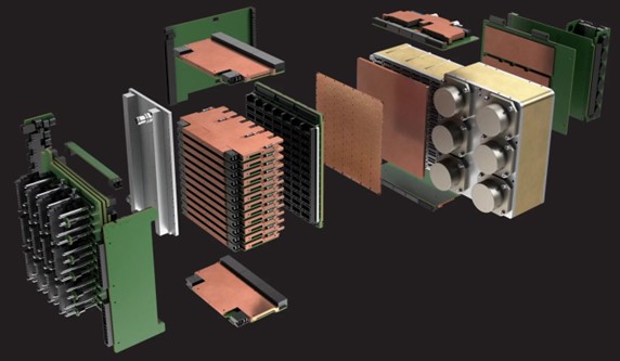
Figure 3: Exploded view of the “Engine Block” at the heart of the Cerebras CS-2 system. Source: Cerebras Systems.
圖3:腦CS-2系統中心的“發動機塊”的爆炸視圖。資料來源:腦系統。
With all this attention to massive integration (putting everything on one giant chip and packaging it efficiently) a typical Cerebras system is about 1/10th the size of an equivalent computer system using the "ancient ways" of wiring up hundreds of thousands of chips together on separate circuit boards, in separate cabinets, and then wiring those together. When asked why he did not favor using multiple small processors in his supercomputers, legendary computer designer Seymour Cray quipped, “What would you rather have pulling your plow? One large bull or 64 chickens?”
所有這些都關注大規模整合(將所有東西放在一個巨大的芯片上並有效地包裝),一個典型的腦系統使用了相當計算機系統的大小的1/10,使用數十萬芯片的“古老方式”在單獨的電路板上,在單獨的櫥櫃中,然後將它們交織在一起。當被問及為什麼他不喜歡在超級計算機中使用多個小型處理器時,傳奇的計算機設計師西摩·克雷(Seymour Cray)打趣道:“您寧願拉什麼犁?一隻大公牛還是64隻雞?”
So what are these trillions of transistors in the WSE used for, you're wondering?
那麼,您想知道的WSE中這些數万億美元的晶體管是什麼?
The killer app of the WSE for AI is in reducing neural network training time—the networks that make AI "intelligent." The WSE can take something that takes other computers weeks and get results in minutes.
WSE的殺手應用程序正在減少神經網絡訓練時間,即使AI“智能”的網絡。 WSE可以花幾週的時間花費其他計算機並在幾分鐘內獲得結果。
The result of this gigantic reduction in training time means answers to AI-powered experiments can come in minutes or hours, not days. This speeds up drug discovery, can model potential cures for cancer, do image processing and work in dozens of new AI-inspired applications that our world will need to face the challenges of the future.
減少訓練時間的巨大減少的結果意味著可以在數分鐘或幾個小時內,而不是幾天來對AI驅動的實驗的答案。這加快了藥物發現的速度,可以模擬癌症的潛在治療方法,進行圖像處理並在數十種新的AI啟發的應用中工作,而我們的世界將需要面對未來的挑戰。
Since so much of the world to come will be shaped by AI-based technologies as time goes by, the WSE is a great milestone to collect, which is why the Museum was particularly happy to bring an example of this amazing device into its permanent collection. The WSE was on display for a limited time at CHM.
由於隨著時間的流逝,將會由基於AI的技術來塑造世界的大部分地區,因此WSE是一個很好的收集的里程碑,這就是為什麼博物館特別樂意將這種驚人設備的例子帶入其永久收藏中的原因。 WSE在CHM上展出了有限的時間。
Blogs like these would not be possible without the generous support of people like you who care deeply about decoding technology. Please consider making a donation.
如果沒有像您這樣的人的慷慨支持,他們深切關心對技術的解碼。請考慮捐款。