Intel Shows Off Work on Next-Gen Glass Core Substrates, Plans Deployment Later in Decade
英特爾展示下一代玻璃核心基板,計畫十年後部署
by Ryan Smith on September 18, 2023 9:01 AM EST作者:Ryan Smith 譯者:美國東部時間 2023 年 9 月 18 日上午 9:01
Although Intel’s annual Innovation event doesn’t kick off until tomorrow, the company is already publishing some announcements ahead of the show – and it’s not the trivial stuff, either. This morning the company is showing off their initial work on developing a glass core substrate and associated packaging process for their chips. As a result of their progress with research and development on the glass cores, Intel is now planning on introducing glass core substrates to its products in the second half of this decade, allowing them to package chips in more complex, and ultimately higher-performing configurations.
雖然英特爾公司的年度創新活動明天才開始,但該公司已經在展會前發布了一些消息,而且這些消息都不是小事。今天上午,該公司展示了他們為晶片開發玻璃芯基板和相關封裝流程的初步工作。由於在玻璃內核研發方面取得的進展,英特爾目前正計劃在本世紀下半葉將玻璃內核基板引入其產品中,使他們能夠將晶片封裝成更複雜、最終性能更高的配置。
There’s a lot to unpack from Intel’s relatively short announcement, but at a high level, glass core substrates have been under research across the industry for over a decade as a replacement for organic substrates, which are widely used in current-generation processors. Essentially the medium that typical silicon dies sit on, substrates play an important part in chip packaging. First and foremost, they provide the structural stability for a chip (silicon dies are quite fragile and flimsy), and they are also the means through which signals from silicon dies are carried, either to other on-package dies (i.e. chiplets), or to the large number of relatively sizable pins/pads on the back side of a chip. And, as chip sizes have increased over the years – and the number of pins/signals required by high-end chips has, as well – so has the need for newer and better materials to use as a substrate, which is what’s been driving Intel’s latest accomplishment.
從英特爾相對簡短的聲明中可以看出很多東西,但從高層次來看,玻璃芯基板作為目前新一代處理器廣泛使用的有機基板的替代品,已經在業界進行了十多年的研究。基板本質上是典型矽晶片所處的介質,在晶片封裝中發揮重要作用。首先,基板為晶片提供了結構穩定性(矽晶片相當脆弱和輕薄),同時也是矽晶片訊號的傳輸方式,訊號可以透過基板傳輸到其他封裝內晶片(即晶片組),也可以透過基板傳輸到晶片背面大量相對較大的接腳/焊盤。隨著晶片尺寸逐年增大,高階晶片所需的接腳/訊號數量也在增加,因此需要更新、更好的材料作為基板,這也是英特爾最新成就的驅動力。
Ultimately, what Intel is aiming to do with glass core substrates is to improve upon what can be done with existing organic substrates, allowing for larger chips with more signals to be routed through the substrate more cleanly. And while this will potentially have benefits for all chips over a long enough time, the immediate focus is on high-end, multi-chiplet processors, where glass core substrates will offer better mechanical stability, better signal integrity, and the ability to more easily route a larger number of signals through a non-silicon medium. In short, Intel considers it one of the keys to making high-performance processors in the next decade.
歸根結底,英特爾使用玻璃芯基板的目的是改進現有有機基板的性能,使更大的晶片和更多的訊號更乾淨地通過基板。雖然在足夠長的時間內,這可能會為所有晶片帶來好處,但目前的重點是高階多晶片處理器,玻璃芯基板將提供更好的機械穩定性、更好的訊號完整性,以及更容易透過非矽介質路由更多訊號的能力。簡而言之,英特爾認為這是未來十年製造高效能處理器的關鍵之一。
Substrates: A Quick Recap
基質:快速回顧
The need for substrates goes back to some of the earliest days for large-scale integrated chips, where chip designs reached thousands and tens of thousands of transistors. These small transistors needed to be wired to much larger pins in order to be installed in systems by relatively massive human hands, leading up to the first chip packages, such as dual in-line packages. These used a frame – typically a lead frame – to hold the actual silicon die, with the frame (or alternatively, wire bonds) providing the signal paths between the die and external pins.
對基板的需求可以追溯到最早期的大規模整合晶片,當時晶片設計的晶體管數量達到數千甚至數萬個。這些小電晶體需要連接到大得多的引腳上,以便用相對龐大的人手將其安裝到系統中,這就產生了最早的晶片封裝,如雙列直插式封裝。這些封裝使用框架(通常是引線框架)來固定實際的矽晶片,而框架(或線鍵)則提供晶片和外部引腳之間的訊號路徑。
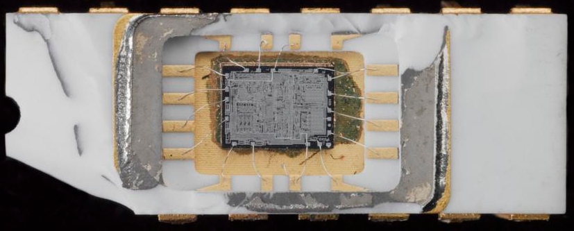
Intel 4004 Delidded (Image Courtesy Science Museum Group Collection Online - CC BY-SA 4.0)
英特爾 4004 Delidded(圖片來源:科學博物館集團線上收藏 - CC BY-SA 4.0)
Since the 70s, there have been several evolutions in substrate designed. Metal frames gave way to classic ceramic chip in the 90s, and then organic packaging around the turn of the millennium. Each iteration of substrate had better properties than the last, above all else, making it easier to route a larger number of signal and power pins to increasingly complex dies.
自 1970 年代以來,基底設計經歷了多次演變。 90 年代,金屬框架讓位給經典的陶瓷晶片,而到了千禧年前後,又出現了有機封裝。每一代基板都比上一代具有更好的性能,最重要的是更容易將更多的訊號和電源引腳連接到日益複雜的晶片上。
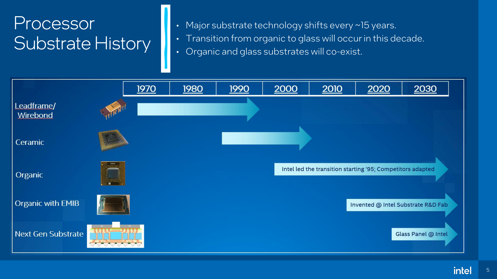
While you’ll still find lead frame and ceramic chips here and there, organic substrates have been the bread and butter of the industry for the last couple of decades. The organic material, essentially made of PCB-like material layered with woven glass laminates, allows for a fairly large number of signals to be routed through a chip, including basic chiplet designs such as Intel’s mobile processors (with PCH separate PCH and CPU dies) as well as AMD’s chiplet-based Zen processors.
雖然鉛框和陶瓷晶片仍時有發生,但在過去的幾十年裡,有機基板一直是業界的麵包和奶油。這種有機材料主要由類似PCB 的材料與玻璃編織層壓板層疊而成,可以在晶片中傳輸大量訊號,包括基本的晶片設計,如英特爾的移動處理器(PCH 與CPU 晶片分離)以及AMD 基於晶片的Zen 處理器。
But organic substrates have already been a limiting factor for some time now, especially in high-end chips. Which is why over the last decade we’ve seen the rise of ultra-high-density interconnect interfaces such as silicon interposers (chip on wafer on substrate), and their derivatives like Intel’s own EMIB. These have allowed companies to bridge together the critical paths of their chips with fast and dense pieces of silicon, but at fairly high costs, and without entirely resolving the drawbacks of organic substrates. As a result, Intel has also been searching for a true replacement for organic substrates, one that will play nicely with large chips, and while not replacing the need for CoWoS/EMIB at the highest level, would offer better signal performance and denser routing than organic substrates today.
但是,有機基板已經成為限制因素有一段時間了,尤其是在高階晶片中。這就是為什麼在過去的十年中,我們看到了超高密度互連接口的興起,如矽內插件(晶片上晶片、基板上晶片)及其衍生產品,如英特爾自己的 EMIB。這些技術使公司能夠用快速、高密度的矽片橋接晶片的關鍵路徑,但成本相當高,而且沒有完全解決有機基板的缺點。因此,英特爾也一直在尋找有機基板的真正替代品,這種替代品可以很好地與大型晶片配合使用,雖然不能在最高級別上取代對CoWoS/EMIB 的需求,但可以提供比目前的有機基板更好的訊號性能和更密集的路由。
Glass Core Substrates: Finer, Yet Stronger
玻璃芯基板:更精細、更堅固
This brings us to the topic of today’s announcement from Intel, glass core substrates. The company has been working on replacing organic substrates with glass for over a decade now, and they’ve finally reached the point of progress where they’re ready to show it off to the world while planning for its use in future products.
這就引出了英特爾今天宣布的主題--玻璃核心基板。十多年來,該公司一直致力於用玻璃取代有機基板,現在終於取得了進展,可以向全世界展示,並計劃在未來的產品中使用。
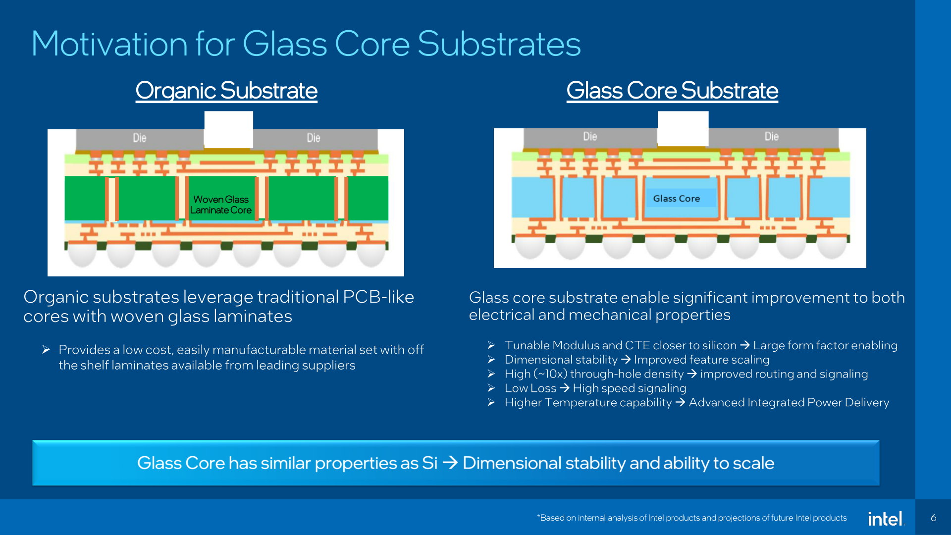
At a high level, a glass core substrate is just that: replacing the organic, PCB-like material of an organic package with glass. To be sure, this doesn’t mean replacing the entire substrate with glass – so Intel is not going to be mounting chips on pure pieces of glass – but rather, the material at the core of the substrate would be made of glass. Meanwhile, metal redistribution layers (RDLs) would still be present on both sides of a chip, providing the actual pathways between various pads and solder joints.
從高層次上講,玻璃芯基板就是:用玻璃取代有機封裝中類似印刷電路板的有機材料。當然,這並不意味著用玻璃取代整個基板--因此英特爾不會把晶片安裝在純玻璃片上--而是基板的核心材料將由玻璃製成。同時,金屬再分佈層(RDL)仍將存在於晶片的兩面,為各種焊盤和焊點之間提供實際的通道。
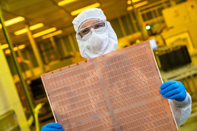
Glass Core Substrates In Panel Form
面板形式的玻璃芯基板
While harder to work with than the now well-established organic substrate, Intel considers glass substrates to be superior both in mechanical and electrical properties, which in turn makes them desirable to use in future chips. Or, conversely, less undesirable than organic substrates when building very large chips.
雖然玻璃基板比現在成熟的有機基板更難加工,但英特爾認為玻璃基板在機械性能和電氣性能方面都更勝一籌,因此更適合用於未來的晶片中。反過來說,在製造超大型晶片時,玻璃基板也沒有有機基板那麼不理想。
Starting from the mechanical side of matter, Intel reports that glass core substrates offer far better mechanical strength than organic substrates. They’re able to withstand higher temperatures better than organic substrates during packaging, resulting in less warping and distortion. Glass is also reportedly easier to get flatter as well, which makes packaging and lithography easier. Finally, glass has a similar coefficient of thermal expansion as silicon (unlike organic substrates), meaning that what little warping that still occurs from heat is consistent with the dies above, as opposed to having different parts of a chip expanding at different rates.
英特爾報告稱,從機械方面來看,玻璃芯基板的機械強度遠高於有機基板。在封裝過程中,它們能比有機基板更好地承受更高的溫度,從而減少翹曲和變形。據報道,玻璃也更容易變平,從而使包裝和光刻變得更容易。最後,玻璃的熱膨脹係數與矽相似(與有機基板不同),這意味著因受熱而產生的微小翹曲與上述模具一致,而不是晶片的不同部分以不同的速度膨脹。
Most importantly, perhaps, is that all of those items taken together open the door to producing larger chips. With a more stable substrate to mount the dies on, it will be possible to have larger dies and a larger number of dies all sharing a single substrate – and thus behaving as a single chip.
最重要的也許是,所有這些項目加在一起,為生產更大的晶片打開了大門。有了更穩定的基板來安裝晶片,就有可能生產出更大的晶片和更多的晶片,所有這些晶片都共用一個基板,從而表現為一個晶片。
Bridging the gap between mechanical and electrical, according to Intel, they’re also able to achieve a much tighter pitch on the through-glass vias (TGVs) that carry signals through the substrate itself, allowing for a much larger number of vias overall. Intel is reporting that they’re able to space TGVs less than 100 microns (µm) apart, allowing for a 10-fold improvement in TGV density. All of which ultimately allows for more flexibility in routing signals through the substrate core, and to some extent makes it easier to route signals with fewer RDL layers.
據英特爾公司稱,為了縮小機械和電氣之間的差距,他們還能在透過基板本身傳輸訊號的玻璃通孔(TGV)上實現更緊密的間距,使通孔的總體數量大大增加。根據英特爾公司報告,他們能夠將 TGV 的間距控制在 100 微米(µm)以內,從而將 TGV 密度提高了 10 倍。所有這一切最終使得透過基板內核佈線訊號時更加靈活,並在一定程度上減少了 RDL 層數,使佈線訊號更加容易。
Assembled Test Chip Substrates
組裝好的測試晶片基板
All of this, in turn, allows for not only larger chips, but for more dies to be placed on a same-sized chip. According to Intel, glass packaging would allow them to place 50% more dies on a chip – or rather, the die complex area within a chip could be 50% larger – allowing for more densely packed chips than what Intel can do today.
反過來,所有這些不僅使晶片的尺寸更大,而且可以在相同大小的晶片上放置更多的晶片。據英特爾公司稱,玻璃封裝可以使他們在晶片上多放置 50%的晶片,或者說,晶片內的晶片複合區可以擴大 50%,從而使晶片的密度比英特爾目前所能做到的更高。
Finally, on the electrical side of matters, glass core substrates, and more specifically the TGVs, reportedly offer better electrical performance as well. Owing to the low loss nature of the dielectric used in TGVs combined with the much larger number of them, Intel says that glass core substrates will allow for cleaner signal routing and power delivery. In the case of the former, that means being able to do 448G signaling through copper, rather than having to use optical interconnects. Meanwhile, lower-loss power delivery would improve overall chip efficiency by that much more, by reducing the amount of energy that is lost as heat before it even reaches the processor dies.
最後,在電氣方面,玻璃芯基板,特別是 TGV,據說也能提供更好的電氣性能。英特爾表示,由於 TGV 所用介質的低損耗特性,再加上 TGV 數量更多,玻璃芯基板可以實現更簡潔的訊號路由和電力傳輸。就前者而言,這意味著可以透過銅纜傳輸 448G 訊號,而不必使用光纖互連。同時,更低損耗的電力傳輸可以減少在到達處理器晶片之前以熱量形式損失的能量,從而大大提高晶片的整體效率。
Farther down the line still, glass core substrates should also make co-packaged optics easier to accomplish for when you do want to use optical. A glass substrate would allow for optical interconnects to be integrated right into the chip, rather than having to tack it on in other manners.
在更遠的未來,玻璃芯基板也將使光學元件的協同封裝更容易實現,以便在確實需要使用光學元件時使用。玻璃基板可以將光學互連裝置直接整合到晶片中,而不必以其他方式貼上去。
So if glass is so great, what’s the catch? While Intel is understandably more excited to talk about what’s good about glass core substrates and what they’ve found works well thus far, one inescapable element will be cost. Like any new technology, glass core substrates will be more expensive to produce and package with than tried and true (and cheap) organic substrates. And while Intel isn’t talking about yields this far out, it will be hard for glass to compete with organic, at least at first.
那麼,如果玻璃如此出色,又有什麼問題呢?可以理解的是,英特爾公司更熱衷於談論玻璃芯基板的優點以及他們迄今為止發現的行之有效的方法,但有一個無法迴避的因素就是成本。與任何新技術一樣,玻璃芯基板的生產和封裝成本將高於久經考驗的(廉價的)有機基板。雖然英特爾並沒有在這麼長的時間內討論產量問題,但至少在一開始,玻璃將很難與有機材料競爭。
More broadly speaking, glass core substrates also means that Intel needs to bootstrap a complete ecosystem for the material. They aren’t vertically integrated with organic substrates today, and they won’t be vertically integrated with glass, either. To that end, Intel is already working with partners today to develop the necessary tooling and supply capacity, to bring themselves to initial commercial production. But over the longer-term, Intel will need to figure out how to make outsourced testing and assembly possible, especially as Intel plans to offer glass core substrates to IFS customers in the future.
更廣泛地說,玻璃芯基板也意味著英特爾需要為這種材料建立一個完整的生態系統。今天,他們還沒有垂直整合有機基板,將來也不會垂直整合玻璃基板。為此,英特爾目前已經在與合作夥伴合作,開發必要的工具和供應能力,以實現初步的商業化生產。但從長遠來看,英特爾需要想辦法使外包測試和組裝成為可能,尤其是英特爾計劃在未來向 IFS 客戶提供玻璃芯基板。
Finally, it bears noting that while glass core substrates allow for a tighter signal pitch than organic substrates, they are not a replacement for EMIB, Foveros, or other more advanced packing techniques based around using silicon mediums. A 75µm pitch for a TGV is still a far cry from the 45µm pitch of EMIB, never mind the <10µm pitch planned for Foveros Direct. So all of those packaging technologies will remain complementary add-ons to glass core substrates, at best replacing EMIB in fringe cases of products that don’t need the full density improvements of EMIB.
最後,值得注意的是,雖然玻璃芯基板可以實現比有機基板更小的訊號間距,但它們並不能取代 EMIB、Foveros 或其他基於矽介質的更先進封裝技術。 TGV 的 75 微米間距與 EMIB 的 45 微米間距相比仍有很大差距,更不用說 Foveros Direct 計劃採用的 <10 微米間距了。因此,所有這些封裝技術仍將是玻璃芯基板的補充性附加技術,最多只能在不需要 EMIB 全面提高密度的邊緣產品中取代 EMIB。
Glass In Action: Intel’s Fully Functional Test Chip
玻璃在行動英特爾全功能測試晶片
The final part of today’s announcement from Intel is based around the manufacturing side of matters. As noted earlier, Intel has been working on glass core substrates for over 10 years now, and more recently has been embarking on a three-and-a-half-year pathfinding project to bring glass core substrates to the next step. Backing those efforts, at this point the company has a fully integrated R&D line up and running in one of their Chandler, Arizona fabs (the same one that does EMIB). Altogether, Intel has spent over a billion dollars on glass core R&D thus far.
英特爾今天宣布的最後一部分是關於製造方面的。如前所述,英特爾開發玻璃芯基板已有十多年的歷史,最近又開始了為期三年半的探路項目,旨在將玻璃芯基板帶入下一個階段。在這些努力的支持下,該公司目前已在亞利桑那州錢德勒的一家工廠(即生產 EMIB 的工廠)建立並運行了一條完全整合的研發生產線。迄今為止,英特爾在玻璃芯研發上的總投入已超過 10 億美元。
The first fruit of their R&D efforts, Intel has completed the assembly of a set of test vehicles – multi-chip packages built over a glass substrate. The chips, which look similar to Intel’s ultra-low power mobile chips (Alder Lake-U 9W?), are reportedly fully functional, giving Intel some practical results to report on. While we don’t have a ton of details on the chip, Intel has told us that it uses 3 layers of RDL, and the TGVs have a pitch of 75µm.
作為研發工作的第一個成果,英特爾已經完成了一組測試車輛的組裝--在玻璃基板上建造的多晶片封裝。這些晶片看起來與英特爾的超低功耗移動晶片(Alder Lake-U 9W?)雖然我們沒有關於該晶片的大量細節,但英特爾告訴我們,它使用了 3 層 RDL,TGV 間距為 75µm。
Along with proving the electrical properties of glass, the small test chip is also intended to prove some of the physical properties, as well. The glass core was made very thick – on the order of 1mm – in order to prove that TGVs would work with such a thick core. For the kind of massive, high-end chips Intel is planning on using glass core packing for, those chips will require a very thick core in order to hit their size goals, so Intel needed to prove that TGVs would (still) work at such lengths.
除了證明玻璃的電氣特性外,這個小型測試晶片還旨在證明一些物理特性。玻璃內核做得非常厚,大約有 1 毫米,目的是證明 TGV 可以使用這麼厚的內核。對於英特爾計劃使用玻璃內核封裝的大型高端晶片而言,這些晶片需要非常厚的核心才能實現其尺寸目標,因此英特爾需要證明 TGV 在這樣的長度下(仍然)可以工作。
Intel Glass Core Substrates: Coming Later This Decade
英特爾玻璃芯基板:將於本十年稍後推出
Wrapping things up, today’s announcement serves as a kick-off of sorts for Intel’s glass core substrate era. Following on their decade of R&D work and their pathfinding sprint, Intel now believes they are ready to begin planning for the transition to glass core substrates in their products – albeit a transition that is still several years out.
綜上所述,今天的公告為英特爾的玻璃芯基板時代拉開了序幕。經過十年的研發工作和探路衝刺,英特爾現在相信,他們已經準備好開始計劃在其產品中過渡到玻璃芯基板--儘管這一過渡仍需數年時間。
If Intel’s product development goes according to plan, the company intends to begin shipping glass core products later this decade. The first products to get the glass core substrate treatment would be their largest and most profitable products, such as high-end HPC and AI chips. These are the products most strained by the use of organic substrates today due to the size limits those substrates impose, and those are the limits intel believes would most benefit from glass core packaging.
如果英特爾的產品開發按計劃進行,該公司打算在本十年晚些時候開始出貨玻璃芯產品。首批採用玻璃芯基板的產品將是其最大、利潤最高的產品,如高階高效能運算和人工智慧晶片。由於有機基板的尺寸限制,這些產品是目前使用有機基板最吃力的產品,而英特爾認為這些產品將最受惠於玻璃芯封裝。
Longer-term, the plan is to waterfall down the technology from HPC chips into smaller and smaller chips, until the technology is available (and viable) for Intel’s rank and file consumer chips. The company is very quick to note that glass and organic substrates will co-exist for years to come – and, like past transitions, there will likely still be chips using organic substrates well after glass is introduced – but the company is also optimistic that they’ll be able to bring the costs of glass core substrates down to parity with organic substrates, eventually making it possible to reap the benefits even in lower-priced processors.
從長遠來看,英特爾的計畫是將這項技術從高效能運算晶片逐步應用到越來越小的晶片中,直到英特爾的普通消費性晶片也能使用這項技術(而且是可行的)。該公司很快就指出,玻璃基板和有機基板將在未來幾年內並存--和過去的過渡一樣,在玻璃基板推出之後,可能仍會有使用有機基板的晶片出現--但該公司也樂觀地認為,他們將能把玻璃核心基板的成本降低到與有機基板相當的水平,最終使低價處理器也能從中獲益。
And Intel won’t be keeping the technology to themselves, either. As part of the company’s broader initiative to become a world class contract foundry, Intel will be offering glass core substrates to IFS customers in due time. While it’s far too early to guess when that would be (even Intel products may be 6 years out), being able to offer glass packaging could give Intel a big leg up over its competitors, especially for producing high-end, highly-profitable chips.
英特爾也不會獨享這項技術。作為公司成為世界級合約代工廠的更廣泛計劃的一部分,英特爾將在適當的時候向 IFS 客戶提供玻璃芯基板。雖然現在猜測具體時間還為時過早(即使是英特爾的產品也可能在 6 年之後),但能夠提供玻璃封裝將使英特爾在競爭中處於有利地位,尤其是在生產高端、高利潤晶片方面。
Above all else, it needs to be reiterated that there’s a great deal of work Intel still needs to do in order to bring glass core substrates to the market. But if the company is successful, then the switch to glass will usher in the kind of major technology transition that only happens every 15 to 20 years.
需要重申的是,英特爾要將玻璃芯基板推向市場,還有大量工作要做。但如果該公司取得成功,那麼向玻璃的轉換將帶來每 15 到 20 年才會發生一次的重大技術轉型。


16 Comments 16 則評論
View All Comments 查看所有評論
FWhitTrampoline - Monday, September 18, 2023 - link
Maybe call that a Glass Interposer instead as that's what that in fact is! So the Traces density on Glass as opposed to Organic Substrate(PCB like material).FWhitTrampoline - 2023 年 9 月 18 日星期一 - 鏈接
也許可以稱之為 "玻璃中間膜"(Glass Interposer),因為它實際上是玻璃中間膜!因此,相對於有機基板(類似印刷電路板的材料),玻璃上的痕跡密度較大。
edzieba - Tuesday, September 19, 2023 - link
It's not an interpose. The wafer is integrated onto the substrate in the same way as any other flip-chip process, not in the wafer-to-wafer bonding of a Si interposer.edzieba - 2023 年 9 月 19 日星期二 - 鏈接
這不是中間膜。晶圓與基板的整合方式與其他倒裝晶片製程相同,而不是採用矽內插的晶圓與晶圓黏合方式。
xol - Monday, September 18, 2023 - link
Suprised no mention of Silicon Nitride which has all the good properties of glass, plus even closer thermal expansion coefficient to silicon, AND excellent thermal conductivity.xol - 2023 年 9 月 18 日星期一 - 鏈接
氮化矽具有玻璃的所有優良特性,其熱膨脹係數甚至更接近矽,而且導熱性能極佳,但奇怪的是沒有提到氮化矽。
Kamen Rider Blade - Monday, September 18, 2023 - link
Interesting, how far along is Silicon Nitride as a PCB substrate?Kamen Rider Blade - 2023 年 9 月 18 日星期一 - 鏈接
有趣的是,氮化矽作為印刷電路板基材的發展程度如何?
xol - Tuesday, September 19, 2023 - link
i dunno.. but as a material it's in common use in semiconductor processes, so...xol - 2023 年 9 月 19 日星期二 - 鏈接
我不知道......但作為一種材料,它在半導體工藝中被普遍使用,所以......
Starfishprime79 - Tuesday, September 19, 2023 - link
SiN has poor electrical properties, specifically very high Dk. Why glass is superior.Starfishprime79 - 2023 年 9 月 19 日星期二 - 鏈接
氮化矽的電氣性能很差,特別是 Dk 值很高。為什麼玻璃更勝一籌?
Kevinlangford - Monday, September 18, 2023 - link
couple more tubes of thermal paste should do the trick!Kevinlangford - 2023 年 9 月 18 日星期一 - 鏈接
多用幾管散熱膏就能解決這個問題!
Dante Verizon - Monday, September 18, 2023 - link
Intel has become a company of promises, I tend not to believe anything they announce that they will achieve in the future.但丁-威瑞森 - 2023 年 9 月 18 日星期一 - 鏈接
英特爾已經成為一家信口開河的公司,他們宣布的任何未來目標我都不會相信。
name99 - Monday, September 18, 2023 - link
Your annual reminder that when Intel announces a tech, it does NOT mean that Intel is the only company with that tech, or even first with that tech; just that Intel has the loudest megaphone.name99 - 2023 年 9 月 18 日星期一 - 聯繫
你每年都要提醒自己,當英特爾宣布一項技術時,並不意味著英特爾是唯一擁有該技術的公司,甚至也不意味著英特爾是第一家擁有該技術的公司;只是英特爾擁有最響亮的傳聲筒。
Other companies are also working on glass substrates and (assuming the Japanese translation is accurate...) https://eetimes.itmedia.co.jp/ee/articles/2210/25/... Apple is already using a version as the substrate for the A16.
其他公司也在開發玻璃基板和(假設日文翻譯準確的話...)https://eetimes.itmedia.co.jp/ee/articles/2210/25/...蘋果公司已經在使用一種玻璃作為A16 的基板。
edzieba - Tuesday, September 19, 2023 - link
That's just Apple's marketing department at work. "Epoxy glass substrate " is the organic substrate everyone has been using for decades.edzieba - 2023 年 9 月 19 日星期二 - 鏈接
這只是蘋果公司行銷部門的工作。 "環氧玻璃基板 "是大家使用了幾十年的有機基板。